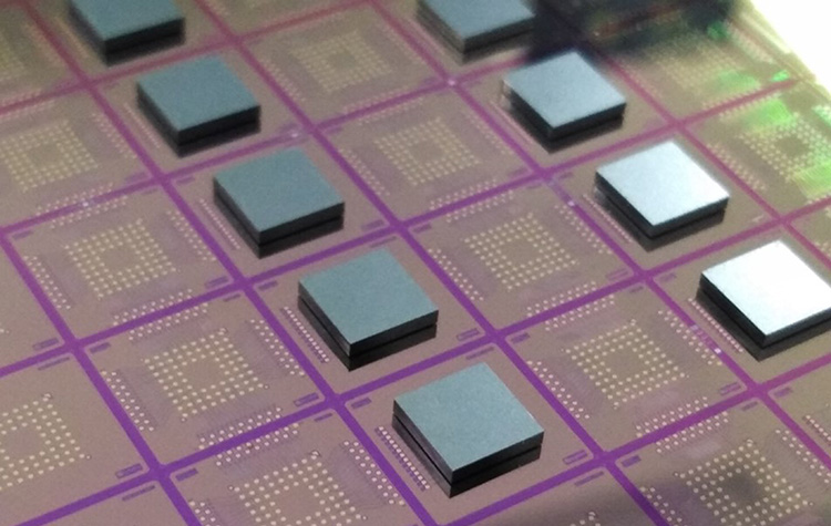
CEA-Leti scientists have opened a pathway to large-scale integration of silicon-spin, or Si-spin qubits, using existing flip-chip processes with die-to-wafer 3 dimensional-interconnect technologies developed in-house, according to a news release.
In a paper presented during the Electronics System-Integration Technology Conference (ESTC), the team reported preliminary electrical characterizations at cryogenic temperatures of chip assemblies made with 3-dimensional interconnects such as SnAg –tin and silver — microbumps and direct Copper (Cu) bonded pads from Cu/SiO2 hybrid bonding process.
The project set out to validate the use of these existing die-to-wafer processes, developed at CEA-Leti, to build interconnects that reliably operate at temperatures lower than 1K, at which quantum bits (qubits) optimally operate. The main goal was to qualify the mechanical and electrical behaviors of these interconnects at the operating conditions required for Si-spin qubit devices and to set references for electrical resistance data to allow further system design.
The project also marked the first time a packaging strategy of quantum devices has been demonstrated with interconnects compatible with large-volume production without the use of indium bumps. Indium bump interconnects are indeed nominally used for applications requiring cryogenic temperatures, such as infrared detectors and, more recently, superconducting qubits. The softness of indium accommodates the mechanical stress created by temperature variation. Fully operational quantum multi-chip assemblies hosting superconducting qubits have even recently been demonstrated by Google and MIT researchers using indium bumps.

Qubits, the building blocks of quantum information, can be made in a broad variety of material systems. But when it comes to the crucial issue of large-scale integration, the range of possible choices narrows significantly. Silicon-spin qubits have a small size and are compatible with CMOS technology. They therefore present advantages for large-scale integration compared to other types of qubits.
“For Si-spin qubits, which are the focus of the Quantum Silicon Grenoble project, there are no strong superconducting requirements for the integration and packaging strategies and so for the choice of the interconnects,” said Candice Thomas, one of the authors of the paper. “The material constraints are less important than for superconducting qubits, thus a wider range of interconnects can be envisioned, such as SnAg microbumps and directly bonded Cu pads from Cu/SiO2 hybrid-bonding processes. SnAg microbumps have the advantage of being widely used in the 3D IC community, and the processes to fabricate them are well known at CEA-Leti with a state-of-the-art pitch as low as 20µm. The motivation to study Cu/SiO2 hybrid bonding lies in its high-resolution potential with a pitch as low as 1µm demonstrated at the institute with a wafer-to-wafer process.”
Achieving Quantum Supremacy
“The reliable operation of these interconnect technologies offers two additional options to hybridize chips with flip-chip processes for quantum computing or any other applications requiring cryogenic temperatures,” Thomas said. “SnAg microbumps and direct Cu bonded pads could be used for different parts of future quantum device packages, depending especially on the needs in terms of pitch and on the type of chips to connect.
This new packaging approach, designed for quantum-chip integration, paves the way for the large-scale integration of qubits, which is necessary to achieve quantum supremacy. Direct bonding will allow us to go a step further in the large-scale integration strategy of Si-spin qubits.”
Achieving quantum supremacy, i.e. demonstrating that a programmable quantum device can solve a problem that no classical computer can solve in any feasible amount of time, requires large-scale integration of quantum bits through 3D architectures functional at sub-Kelvin temperatures.
The CEA-Leti team’s next steps are to use these 3D interconnect technologies to hybridize a chip with qubits to a multichip module and to verify that the interconnects themselves and the associated interconnect fabrication and stacking processes are not affecting or damaging qubit properties.


