Insider Brief
- Researchers at Imec demonstrated superconducting transmon qubits with relaxation and coherence times exceeding 100 microseconds, using a 300mm silicon wafer process.
- The study shows a 98.25% yield of functional qubits, highlighting the viability of industrial methods like optical lithography and reactive-ion etching for scaling quantum processors.
- The researchers plan to integrate more advanced semiconductor techniques and explore three-dimensional architectures to further improve qubit performance and scalability.
- Image: Photograph of the 300 mm wafer. (From the Nature paper)
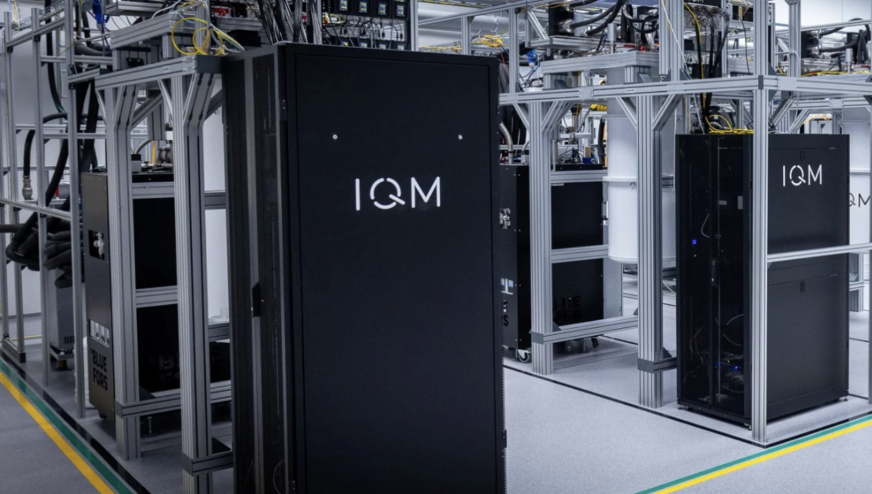
Researchers at Imec, a Belgium-based research center, have demonstrated a new method for fabricating superconducting transmon qubits using a 300mm silicon wafer process, according to a study in Nature.
The study shows that these qubits achieved relaxation and coherence times exceeding 100 microseconds (µs), indicating significant potential for the scaling of quantum processors. The method leverages industrial semiconductor fabrication techniques, such as optical lithography and reactive-ion etching, which are typically not used in quantum computing fabrication but offer greater scalability.
The new approach provides a large-scale, industry-compatible process for creating superconducting qubits, a crucial component of quantum computing. The study reported a 98.25% yield of functional qubits, which suggests the viability of these industrial methods. These qubits demonstrated energy relaxation times (T1) and coherence times that are competitive with conventional lab-based techniques, which are typically more limited in scale.
From Fabrication to Calculations
The successful fabrication of superconducting qubits on a 300mm wafer using standard semiconductor processes is an important step for scaling superconducting quantum computers, the researchers write in the paper. The advance is aimed right at the heart of scalability in quantum computing, a need the researchers acknowledge in the paper.
“In the pursuit of quantum computational advantage and, eventually, fault-tolerant, error-corrected, quantum hardware, a need for more and better physical qubits with high-fidelity control is apparent,” the researchers write. “Advances in error-correcting codes and quantum gate fidelities could reduce the required number of physical qubits. Additionally, increased stability and uniformity of the qubits would reduce the significant control and tuning overhead. However, for practical applications, the number of physical qubits on a quantum computer will most probably still scale beyond a million.”
The qubits’ relaxation times exceeding 100µs is a key measure of their ability to maintain quantum states for longer periods, which would be necessary for practical calculations. According to the researchers, this performance is on par with lab-scale fabrication methods but offers the added benefit of scalability. The study showed consistent performance across the wafer, with high yield and minimal variability, marking a major step toward building larger quantum processors.
The team fabricated Josephson junctions (JJs), a key component of superconducting qubits, using a 300mm complementary metal–oxide–semiconductor-compatible (CMOS) overlap process. These JJs were characterized using scanning electron microscopy (SEM) and transmission electron microscopy (TEM) to confirm their structural integrity. Across the wafer, 393 out of 400 qubits were fully characterized, demonstrating a 98.25% yield of functional qubits. The researchers observed minimal variability in qubit frequencies and relaxation times across the wafer, confirming the reliability of their process.
Vision: Producing Millions of Reliable Qubits
The researchers report this paves the way for large-scale quantum processors, which will likely require millions of physical qubits to achieve practical quantum computing.
The ability to fabricate qubits using industrial methods aligns with the need for scalable quantum hardware, which is essential for quantum error correction and fault-tolerant quantum computing. The high-coherence times demonstrated by the qubits fabricated in this study suggest that these industrial methods could be used to produce reliable qubits for future quantum computers.
The use of standard semiconductor processes, such as optical lithography and reactive-ion etching, offers several advantages. These methods allow for greater process control, higher yield, and scalability compared to the metal lift-off and electron-beam lithography techniques typically used in quantum computing research.
Also of note, the potential for integrating these qubits into three-dimensional architectures could further enhance the complexity and connectivity of quantum processors.
Methods
According to the paper, the researchers obtained their results using the following methods and processes. The qubits were fabricated using an industry-standard 300mm silicon wafer process at Imec’s clean room facility. The process involved patterning each die using an optical mask and replicating the die across the 300mm wafer. Each die contained 20 subdies, featuring different designs of qubits, resonators, and test structures. The Josephson junctions, which form the core of the qubits, were fabricated using an aluminum-aluminum oxide-aluminum (Al/AlOx/Al) overlap process.
The performance of the qubits was evaluated in a dilution refrigerator at a temperature of 10 millikelvin (mK). The researchers measured the qubits’ energy relaxation times (T1) and coherence times using Hahn-echo experiments. The across-wafer variability of the qubit frequencies and Josephson junction resistance was also measured to assess the uniformity of the fabrication process.
Limitations and Future Research
While the results are promising, the researchers indicated some limitations to the current approach, which could then guide future research directions. The researchers identified two-level system (TLS) defects at capacitor interfaces as the dominant source of decoherence, which might impact qubit performance.
The study also noted that further optimization of the Josephson junction fabrication process, particularly in terms of barrier oxidation, would be necessary to improve coherence times further.
According to the paper: “Our variability analysis of the JJ normal resistance and qubit frequency indicated that the current limitation resides in barrier oxidation. However, the area control realized through optical lithography and subtractive dry-etching shows clear promise for further optimizations beyond the state of the art.”
The team reports plans to integrate additional semiconductor processing techniques, like chemical mechanical polishing and silicon trenching, while also exploring three-dimensional integration methods to improve qubit yield, uniformity and connectivity for more complex quantum processors.
The researchers write: “Looking ahead, the qubit fabrication process presented in this work, aligned with CMOS foundry standards, establishes a robust baseline for future enhancements. The integration of industry-standard techniques (such as chemical mechanical polishing, silicon trenching and the deposition of sophisticated material stacks) alongside three-dimensional integration, will provide the necessary yield, uniformity and connectivity needed to fabricate increasingly complex quantum processors.”
The study was conducted by J. Van Damme, S. Massar, R. Acharya, and colleagues at Imec, Leuven, Belgium, with contributions from researchers at the Department of Electrical Engineering (ESAT), KU Leuven.
The work is extremely technical and this summary likely falls short for those looking for a deep understanding of the process — for a deep dive, read the researchers’ work in Nature.