
Insider Brief
- EuQlid has emerged from stealth with $3 million in funding led by QDNL Participations and Quantonation, alongside $1.5 million in early customer revenue, to launch a quantum-based 3D imaging platform for semiconductors and batteries.
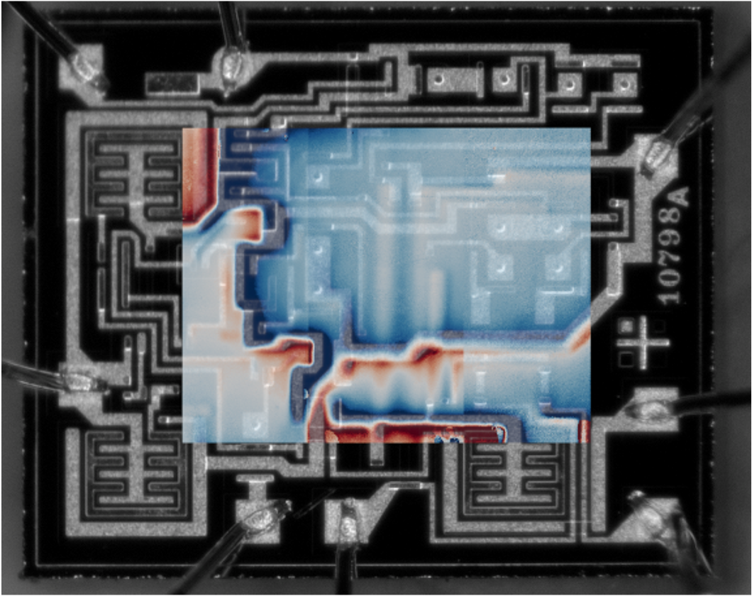
- The company’s Qu-MRI platform uses quantum magnetometry, signal processing, and machine learning to map buried electrical currents non-destructively, addressing inspection challenges in advanced semiconductor and energy-storage manufacturing.
- Founded by physicists and engineers from Harvard, Yale, and the University of Maryland, EuQlid aims to bring quantum precision to industrial-scale metrology, targeting a fast-growing global market for advanced inspection tools exceeding $10 billion annually.
PRESS RELEASE — EuQlid, a quantum technology company developing next-generation design and metrology tools, today announced its emergence from stealth mode with $3 million raised from lead investor QDNL Participations with participation from Quantonation, and over $1.5 million in early customer revenue, to deliver a breakthrough 3D imaging solution for semiconductors and batteries.
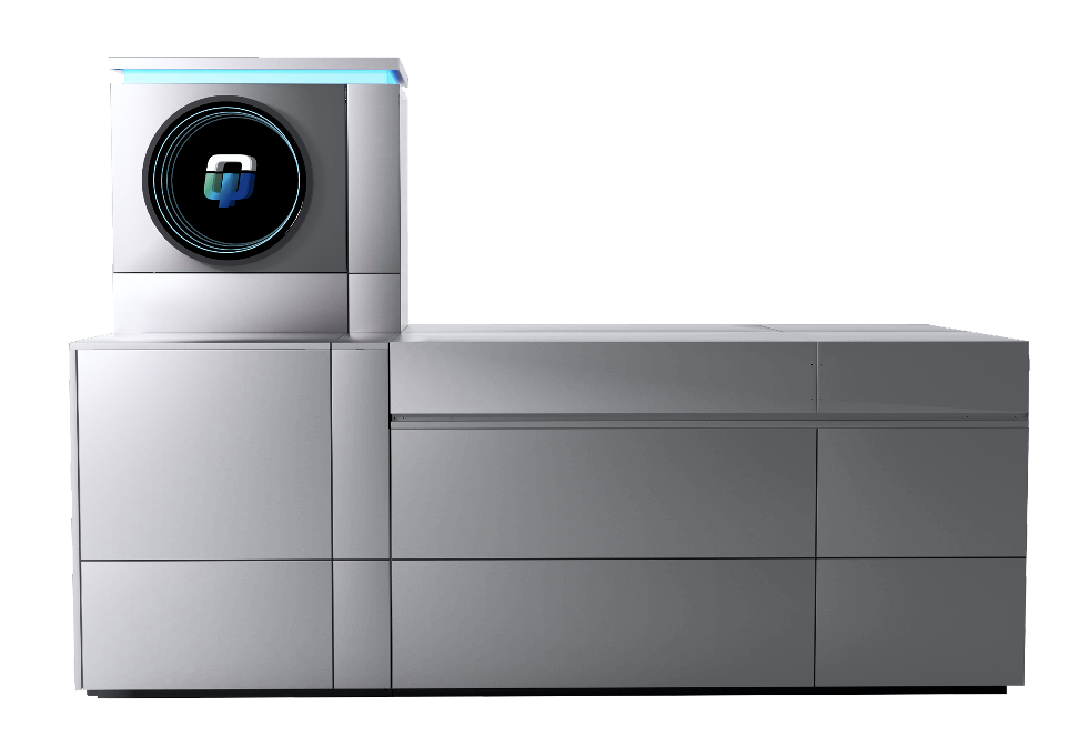
EuQlid’s proprietary quantum imaging platform – Qu-MRITM – enables non-destructive mapping of buried current flow with unprecedented precision inside complex materials and devices.
The company’s quantum-based technology addresses a critical gap in the semiconductor and energy storage industries, visualizing sub-surface currents with precision and speed, where today’s inspection and test tools cannot reach, for new product development and high-volume manufacturing yields.

Multi-Billion Dollar Market Opportunity
The insatiable compute demand of AI is accelerating semiconductor logic, memory and advanced packaging to adopt complex 3D architectures to deliver performance, cost and power. New metrology and inspection tools are required to control and optimize increasingly complex manufacturing workflows. Global demand for advanced metrology and inspection tools exceeds $10 billion annually and is growing rapidly with the adoption of 3D architectures.
“Our mission is simple,” added Sanjive Agarwala, co-founder and CEO. “We want to make quantum precision available now, addressing fundamental 3D metrology and inspection whitespace, to enable the next era of semiconductor and battery revolution.”
Quantum Precision Meets Industrial Scale
The Qu-MRI platform combines quantum magnetometry with advanced signal processing and machine learning to deliver buried electrical current maps with high-throughput and nano-amp sensitivity without physical contact or destructive cross-sectioning. These capabilities provide customers with powerful insights, from spatial analysis of state-dependent power flows in functioning CPUs and GPUs, to the detection and localization of interconnect stacking errors during high bandwidth memory manufacturing. The flexible core technology will drive applications in semiconductors, energy storage, and advanced materials, for both R&D labs and inline manufacturing environments.
“EuQlid’s Qu-MRI addresses a foundational technology need for the design and manufacturing of next-generation semiconductors, by non-invasively visualizing buried connectivity defects,” said Paul van der Heide Ph.D., Materials and Component Analysis Director at Imec.
From Quantum Science to Fab-ready tools
EuQlid was founded by Ronald Walsworth, David Glenn and Sanjive Agarwala, a leading team of physicists and engineers from Harvard, Yale, Univ. of Maryland, Cadence and Texas Instruments, combining deep expertise in atomic physics, quantum sensing and the semiconductor industry.
“We are thrilled to lead the investment round in EuQlid, a company founded by true pioneers of diamond-based quantum sensing and guided by a seasoned semiconductor executive, addressing a critical bottleneck in advancing the next generation of semiconductors and batteries,” said Kris Kaczmarek, Ph.D., Investment Director at QDNL Participations.
“Semiconductor fabrication is a critical and strategic industry, and we are excited for EuQlid’s quantum sensing technology to target a key whitespace to help the sector grow to its next phase,” said Will Zeng, Ph.D., Partner at Quantonation.
First Generation Product Deployed Across the Globe
EuQlid’s first generation Quantum Diamond Microscope (QDM) product for geosciences and bioimaging applications has been delivered worldwide and is in use at Harvard University (USA), New York University (USA), Oxford University (UK), and Curtin University (Australia) among others.
“The now-widespread demand in geosciences for new QDMs demonstrates that it has succeeded spectacularly in this regard. Along the way the capabilities that EuQlid has developed to measure minute magnetic fields at microscopic scales are the perfect launchpad for micro-electronics applications,” said Roger Fu, Ph.D., Professor of Earth and Planetary Sciences at Harvard University.