Dr Matthew Markham and Dr Daniel Twitchen explain how Diamond – a special form of carbon – now has many practical quantum applications.
Diamonds are well known as the gem for marking engagements and other special occasions, but the huge influence of this material in industry is all around us too. Diamond is used, for example, as a tool for machining the latest smartphones, as a window in high-power lasers used to produce automotive components, and even as a speaker-dome material in high-end audio systems. However, there is a new application on the horizon that could be even more profound – that of diamond quantum technologies.
At the turn of the 20th century, theoretical and experimental scientists were grappling to understand how the universe worked at very small scales. The results of this turned into the field of quantum mechanics, which has led to innovations – such as lasers and transistors – that impact our daily lives. These so-called “quantum 1.0” technologies rely on the effects of quantum mechanics, but now in the 21st century, scientists around the world are trying to develop the next wave of innovations. “Quantum 2.0” technology will rely on manipulating and reading out quantum states, and will typically exploit the quantum effects of superposition and entanglement.
The challenge of developing quantum technology is that quantum states are so fragile. Ideally these states would be isolated from everything else, but to make them useful you need to interact with them. Some applications can take advantage of this fragility – for example, in developing highly sensitive sensors – but they still need a degree of isolation to be controlled in the first instance. This balance between control and interaction is the fine line quantum scientists are having to traverse.
Quantum technology research covers quantum computing, simulation, communication and sensing, with potential impacts in healthcare, the automotive industry and the development of new materials, to name a few. Currently a wide range of different technological solutions are being investigated for these new applications, such as trapped ions, superconductors, quantum dots, photons and defects in semiconductors. Each technical solution has different pros and cons. Trapped ions have exquisite quantum properties but are challenging to integrate, whereas circuits of superconductors can be fabricated but can only operate at cryogenic temperatures. This is where materials like diamond come into play as they offer a compromise by being solid-state – making it easier to integrate into devices – and operational at room temperature.
Quantum diamond
A lot of research into diamond has focused on identifying the hundreds of different defects that can be found within the carbon lattice. One such imperfection is the negatively charged nitrogen-vacancy (denoted as NV) defect (see box below). In 1997 Jörg Wrachtrup and colleagues at the University of Technology Chemnitz in Germany showed that a single NV defect could be manipulated and provide an optical output at room temperature (Science 276 2012). This discovery sparked the field of diamond quantum technology (see Nature 505 472 for a more detailed history). The process is called optically detected magnetic resonance (ODMR) and, with the NV defect, it is observed when measuring a change in fluorescence after shining green light on a single NV defect, or on an ensemble of them, while scanning an applied microwave field. When the field hits resonance with the spin quantum numbers (ms) causing a transition from ms = 0 to ms = ±1, a decrease in fluorescence is observed. So by measuring the intensity of the fluorescence, you can read out the spin state of the defect.

Imagine a perfect diamond lattice of repeating carbon atoms. Remove two adjacent atoms, then replace one with nitrogen (bright blue in figure), while the other remains a “void” or vacancy (pale blue). This is the neutral nitrogen-vacancy defect in diamond, and it can have four different crystallographic orientations. Should there be another defect nearby in the lattice that has an electron with higher energy – usually a substitutional nitrogen that has no vacancy – this electron will transfer to the nitrogen-vacancy to give it a negative charge.
The electrons associated with the negatively charged nitrogen-vacancy (NV) defect occupy the dangling bonds around the vacancy such that their energy levels behave similarly to those in a trapped ion.
These NV defects have a special combination of energy levels, such that whatever ground-state spin an electron starts in, once the crystal is illuminated with green light, it will cycle through energy levels and is statistically more likely to enter the spin state ms = 0. Cycle the electrons around this loop enough times and the spins will effectively be aligned. Once in this ms = 0 ground state the NV defect can be manipulated to do a quantum experiment by applying microwaves and further pulses of light. The readout process relies on the same phenomena, exploiting the fact that the amount of light emitted by the defect is “bright” or “dark” depending on its ground-state spin when measured.
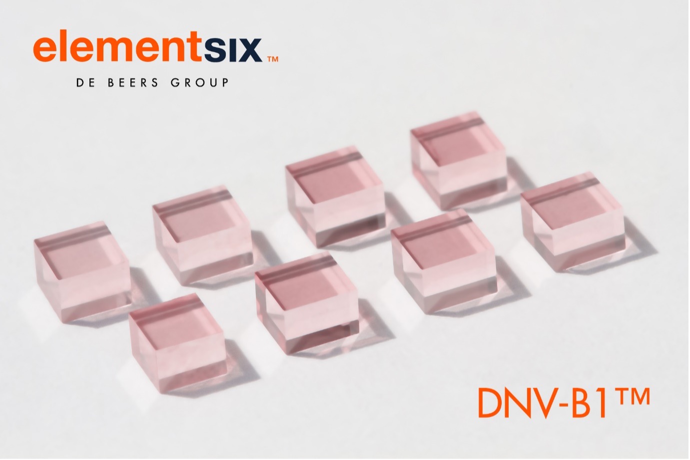
Over the next decade, a few academic groups around the world picked this work up, hoping to use diamond as a quantum bit, or “qubit”, in quantum information devices, such as quantum computers. This work was undertaken using a single, unique natural diamond dubbed the “Magic Russian Diamond”. Meanwhile, many companies began developing new techniques to produce high-purity synthetic single-crystal diamond for industrial applications using microwave-assisted chemical vapour deposition. In the early 2000s, for example, staff at our firm Element Six showed that it was possible to grow diamond with fewer than five impurity atoms per billion carbon atoms. In such diamond, nitrogen is the predominant impurity, and isolated NV centres can be probed. Eventually, in 2006 when this material’s quantum properties were tested, they were shown to be comparable to the Magic Russian Diamond. The finding was significant because the new synthetic diamond could be mass produced (see figure 1) and therefore allowed many more academic groups to have access to the material and start to understand how to control and use the NV defect.

At this point, much of the academic research was focused on fundamental quantum physics and quantum computing. However, in 2008 work taking place in the group of Wrachtrup – who was now at the University of Stuttgart, Germany – and in Mikhail Lukin and Ron Walsworth’s groups at Harvard University in the US, proposed and showed that diamond could be used to make a magnetic sensor, in which the brightness of the NV defects’ optical output depends on the strength of the magnetic field. Since then, many new applications using the NV defect have been proposed.
The reasons why diamond provides such a wonderful host to quantum defects come from its crystal structure. For example, diamond is a wide band-gap material, meaning that it can host a range of defects with transition energies in the optical regime, enabling the defects to be manipulated with readily available lasers. As carbon has a low atomic mass and very stiff interatomic bonds, it has a high Debye temperature (the temperature of a crystal’s highest normal mode of vibration), which makes the interaction of the NV centre with the vibrational modes of the surrounding lattice unusually weak, even at room temperature. Diamond also has a naturally low concentration of nuclear spins (carbon-12 has a nuclear spin of 0 and there is only 1.1% carbon-13 (spin –1/2) in diamond). This reduces the likelihood of the quantum states “decohering”, when the spin is no longer in the desired state. Quantum states can also decohere via spin-orbit coupling – a relativistic effect where the spin of a charge interacts with its orbital motion. But because the NV defect has weak spin-orbit coupling, there is limited decoherence and the spin state lasts for longer. Together, these properties mean that it is possible to fabricate a diamond with a spin decoherence time of milliseconds at room temperature. And as well as diamond being a good host for spin defects, the NV centre is also particularly special in that its electronic energy-level structure means that the electronic spin associated with it can be manipulated simply by shining green light on it.
Despite these desirable features, the NV defect in diamond is not perfect. In an ideal world, all the photons emitted would be at 637 nm for them to be quantum mechanically indistinguishable. However, most of the photons emitted are at different wavelengths, from 637 nm to 800 nm, due to phonon interactions, which provides a challenge for some applications. Other difficulties are that diamond is not as easily processed as materials such as silicon – it is much harder to etch structures in diamond to improve optical collection from the defects, and high-purity single-crystal diamond has only been made up to around 10 mm2. These limitations of diamond and the NV defect have led to scientists looking for alternative defects in diamond and in other wide band-gap materials such as silicon carbide (SiC) and zinc oxide (ZnO). However, while a few other defects in diamond and other materials have been identified to have useful properties, no-one has found one that rivals diamond’s NV centres.
Diamond devices
One of the benefits of a diamond-based quantum device is its simplicity. A basic device can be fabricated from a green light source, a diamond, a small microwave source and a photodetector. This is because effective optical initialization and the readout process of NV spins do not require specialized narrow-linewidth lasers – even a simple green LED can be used. Furthermore, because of the wavelength of light being detected (637–800 nm), low-cost, off-the-shelf silicon photodetectors can be used. An offset magnet is also used to provide a field of a few millitesla, which separates the energy levels of the four different possible crystallographic orientations of the NV defect, allowing them to be probed independently. Lastly, the microwave frequencies that are used are roughly 2880 MHz. All of these components can be bought off the shelf for a few thousand pounds, and instructions to build such a room-temperature quantum device are readily available and suitable for a first-year physics degree demonstration (American Journal of Physics 86 225). However, while this set-up shows the principles of operation, it clearly does not show the enhancements in performance you would expect from a quantum device.
Extensive engineering is required to maximize performance in a particular application. For example, if you require ensembles of NV defects, there is a trade-off in performance between the concentration of NV defects in the diamond and the spin coherence time. If the NV defects are too close together, interactions with nitrogen – which donate the electron to form the negative NV charge state – reduce the spin-coherence time. However, if they are too far apart then it is harder to provide each defect with the same uniform illumination, magnetic field and microwave field, as well as collect as much of the luminescence from the NV defects at the detector.
The original motivations for academic work on diamond-based quantum systems were to investigate fundamental physics and to consider using diamond in a quantum computer. This is the most demanding of all the diamond quantum applications as it requires the most stringent performance of the defects. Specifically, each defect needs to behave in exactly the same way, emitting light at precisely the same wavelength. Unfortunately, imperfections – such as dislocations in diamond’s crystal structure – create strain, which shifts the emission wavelength of the light enough to make two NV defects distinguishable. This can be countered by applying an electric field near a defect that can be “Stark tuned” such that the emission wavelength is the same – however, changes in the local charge configuration surrounding the NV can still change during a measurement causing a wavelength shift. Despite these potential hurdles, several breakthrough results have been achieved with diamond, including the first successful “loophole-free Bell’s inequality test” in 2015 (Nature 526 682), and the longest spin lifetime without the use of any cryogens. Building on these achievements, a 10-qubit register that can store quantum information for up to 75 s has recently been demonstrated (Phys Rev. X 9 031045).
As part of a current project, Ronald Hanson’s group at the Delft University of Technology in the Netherlands is using the NV defect in diamond as a “quantum repeater node” in a 100% secure quantum internet. In such a network, the nodes are quantum mechanically entangled to build up a chain from the source to the receiver so that quantum information can be transmitted over large distances. Such a demonstration is a challenging target, but there are also many nearer-term applications using the fragility of the quantum states.
Another emerging application is the diamond-based maser. Invented in the 1950s, masers are not as widespread as lasers but nevertheless have many invaluable applications. Masers are used in radio astronomy and deep-space communication due to their high gain and very low noise. Being so stable over short timescales, they are also used as oscillators, which enables high-precision timing required for global positioning systems.
However, current maser systems can be bulky and complex, and can also require cryogenics, which limits where they can be deployed. A breakthrough in 2018 (Nature 555 493) demonstrated the world’s first continuous-wave (CW) room-temperature solid-state maser using the NV defect in diamond. This maser works using the same energy levels used in magnetometry but a magnetic field of greater than 0.1 T is applied, which pushes the ms = –1 energy level below the ms = 0 energy level via the Zeeman effect. Choosing a particular magnetic field strength, you adjust the energy gap between the levels and thereby select the operating frequency of the maser. Then, pumping the diamond with a green laser puts the electrons in the ms = 0 energy level and thereby creates a population inversion.
To get maser operation requires the diamond to be in a high Q cavity, the applied magnetic field to be stable and homogenous, and the temperature fluctuations of the diamond to be minimized. If these engineering challenges can be solved, compact diamond masers may pave the way not just for existing maser applications, but also for new opportunities that have yet to be considered due to the limitations of current maser technology.
Detecting with diamonds
As mentioned, in 2008 the concept of using the NV defect in diamond as a magnetic sensor was first proposed, with practical demonstrations appearing in 2009. In a diamond magnetic sensor, the luminescence collected does not have to be at a particular wavelength and therefore all emission in the phonon sidebands from 637 nm to 800 nm can be collected as signal. A diamond magnetic field sensor in principle has many advantages over other sensor technologies. For example, it is an intrinsic vector sensor by virtue of the fact that it is sensitive along the axis of the NV defect, which means that the four different NV orientations can be used to reconstruct a vector field. It also has a massive bandwidth, being sensitive to magnetic fields over several orders of magnitude, and – unlike other technologies such as vapour cells – it does not require special magnetic shielding.
There are also different modalities of NV magnetic sensor depending on how many defects are used in sensing. Due to the NV defects’ properties, strong electronic dipole luminescence from single ones can be easily measured, allowing magnetic fields to be measured on the nanometre scale. Competing technologies such as magnetic resonance force microscopy can also do this, but as they are intrinsically magnetic, they perturb the system they are trying to measure. Many groups are therefore using NV-based tools for material characterization, such as investigating magnetic materials that contain skyrmions. Start-ups such as Qnami, based in Switzerland, are trying to capitalize on these developments by selling ready-made diamond probes containing NV defects.
Using ensembles of NV defects can make the device more sensitive but lower its spatial resolution. As a compromise, a few microns of high-NV-defect-containing diamond on top of a high-purity diamond can be used to image magnetic fields where the thickness of the NV-containing layer determines the spatial resolution. This technique has been used to measure the magnetic signature from a meteorite, which could then be used to establish the magnetic field when the solar system was formed. Adding even more NV defects into the diamond to make a bulk diamond sample containing NV defects throughout can push sensitivities into the picotesla regime.
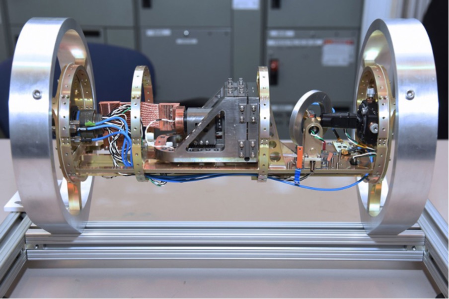
Using such a bulk magnetometer, a team at Lockheed Martin – the US-based aerospace company – has been developing a diamond magnetometer that can be used as an alternative GPS that does not rely on external signals (see figure 2). The technology works by using the vector capability of a diamond magnetometer to sense the strength and direction of Earth’s magnetic field. Given that Earth’s field varies depending on where you are on the surface, this fact can be used to position yourself without relying on an external source that can be jammed. Even early prototype systems have demonstrated this and, while not as accurate as satellite-based GPS, they will likely work alongside existing technology to provide redundancy.
The sensor can also be used in reverse to detect radio-frequency (RF) fields. In this configuration, a magnetic field gradient is placed across the NV-containing diamond in a controlled way, which then provides a known Zeeman shift of the energy levels. When a microwave signal of unknown frequency is applied, a magnetic resonance appears at the position that corresponds to that frequency. The big advantage of this approach is that you can measure across a whole frequency spectrum – more than tens of gigahertz – in one measurement and with high resolution. This technology could be used in 5G networks to prevent interference between neighbouring cell towers.
Diamond-based quantum technology also has applications in the medical industry. A few groups around the world, as well as the start-up NVision based in Germany, are using diamond to enhance magnetic resonance imaging (MRI) – turning it from an anatomical to a molecular imaging modality similar to positron emission tomography (PET). The principle of the technology is to transfer the electronic spin from NV defects to the nuclear spin of a target molecule. The NV defects are placed in close contact with the target molecules and are then illuminated with green light, and a microwave source is also applied. Then, by using a series of microwave pulses, the spin can be transferred from the diamond to the target molecules’ nuclear spin. The nuclear spin lasts long enough to allow the molecules to be administered to the patient and the patient measured in an MRI, where now there is a high degree of spin polarization that gives high contrast in the MRI.
Diamond’s quantum future
Diamond is now well established as a major player in quantum materials, with more than 200 academic groups around the world working on applications of its quantum properties. There is also a growing number of companies developing diamond quantum technology, including large firms such as Lockheed Martin, Bosch and Thales, as well as many start-ups such as Quantum Diamond Technologies, NVision and Qnami. The material is at the heart of all of this technology, but lots of time-consuming engineering is required to make optimized devices. Even so, in many cases, potential customers are already testing prototype systems.
An additional barrier to device development is the learning curve required in getting the most out of the NV defect, which takes a skilled quantum physicist. This is where some of the national and international programmes in the UK, Europe and the US are helping by providing a supply of quantum scientists to organizations that do not have the relevant skills in-house. The final challenge is that it is impossible to say which of the diamond quantum technology applications will result in the most viable markets as the technology itself is so disruptive. So while we do not know how big an opportunity diamond quantum technologies might provide, one thing is clear: they are certainly here to stay.
For more market insights, check out our latest quantum computing news here.