Insider Brief
- C12 has unveiled its proprietary Pick & Place nanoassembly process, designed to transfer individual carbon nanotubes onto silicon chips with high precision for quantum processor manufacturing.
- The company said the process enables preselection and qualification of carbon nanotubes before integration, helping address qubit variability and improve manufacturing control.
- C12 reported that the new approach has significantly increased production throughput and supports the integration of higher-density multi-qubit chip architectures.
PRESS RELEASE — C12, a Paris-based quantum computing company developing carbon nanotube spin qubit processors, today announced its proprietary Pick & Place nanoassembly technology: a custom-built, patented nanoassembly method developed entirely in-house to transfer individual carbon nanotubes onto silicon chips with micrometric precision, in controlled vacuum or inert atmosphere conditions. Two setups are now operational in C12’s Paris laboratory.
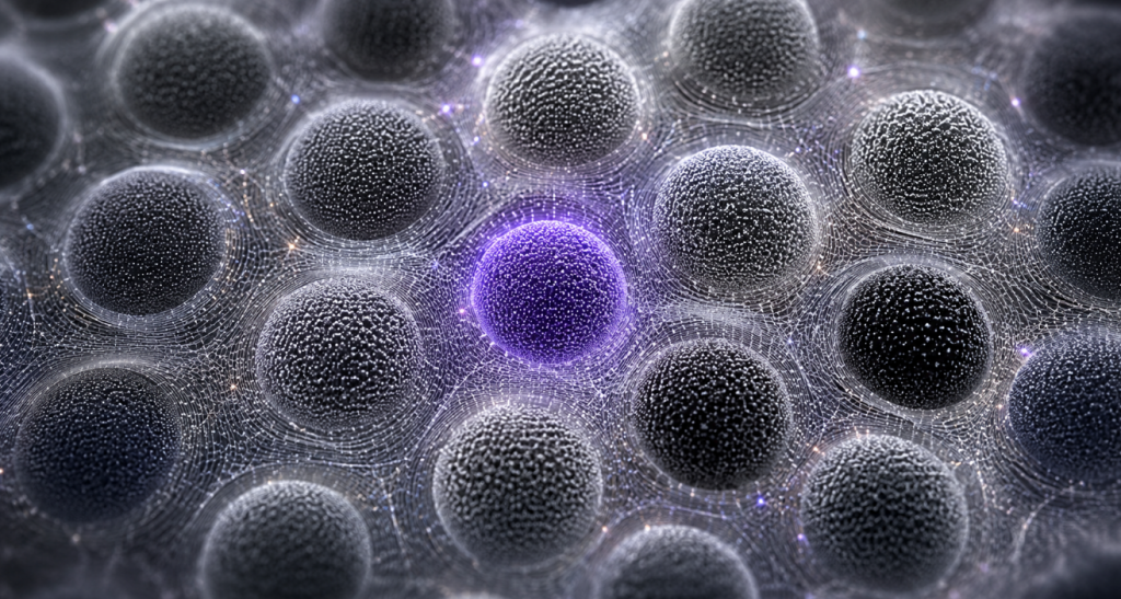
Pick & Place is a core building block of how C12 envisions the scalable manufacturing of carbon nanotube quantum processors. A carbon nanotube is 100,000 times thinner than a human hair — placing one on a chip is like placing a hair on a surface the size of Paris, accurate to within a few streets. By introducing an intermediate assembly step that decouples nanotube growth from chip fabrication, the process brings significantly more flexibility and modularity to C12’s fabrication flow, while addressing one of the hardest challenges in quantum hardware manufacturing: qubit variability.
The process allows C12 to preselect and qualify individual carbon nanotubes before integration, enabling much tighter process control and guaranteeing the quality of the assembled devices. C12 is currently the only company capable of doing this through electrical prescreening at the qubit level.

The throughput numbers illustrate the step change in process maturity. With the process now streamlined and partially automated, C12 assembled 50 devices in the last four weeks. The same number took the entire year of 2025 to assemble using the previous method.
This new manufacturing approach also enables the scaling integration of multi-qubit structures. C12’s High-Density chip integrates 17 quantum devices on a single chip, breaking the ceiling of low CNT count chips, now only limited by the current density of devices on the chip. First announced by Pierre Desjardins at the Q2B conference in San Francisco, the HD chip serves as a proof point that precise multi-nanotube integration is both achievable and repeatable, while C12 continues to perfect its high performance single and two-qubit building blocks.
“Pick & Place is directly inspired by techniques used in advanced semiconductor packaging, where the same concept enables very high throughput integration. We adapted it to the nanoscale to achieve an assembly of carbon nanotubes, opening the same long-term opportunity for quantum chip manufacturing,” said Matthieu Desjardins, co-founder, chairman, and CTO of C12.
Beyond the technical milestone, the technology adds a significant new layer to C12’s IP portfolio alongside existing patents in qubit control, carbon nanotube growth, and quantum device architecture.
The announcement follows C12’s technology roadmap, published in April 2026, which targets four processor generations from Aïdôs (2027) to Panopeia (2033), scaling from a first logical qubit to over 100,000 physical qubits at utility scale. Reproducible manufacturing is one of the core challenges the roadmap must solve. Pick & Place is C12’s answer, built and running today. This milestone completes a broader sequence of progress: material foundations validated through a Nature Communications publication, error correction tooling secured through a partnership with QC Design, and hardware connected to the enterprise software ecosystem through an integration with Classiq. The manufacturing infrastructure to execute the roadmap is now in place.