
Insider Brief
- QuantumDiamonds deployed its QDm.1 quantum sensing system at iST in Taiwan, marking its first installation in Asia and a step toward adoption in high-volume semiconductor failure analysis.
- The system uses Quantum Diamond Microscopy to provide non-destructive, high-resolution 3D imaging of current pathways in advanced chip architectures, helping manufacturers identify defects and improve yields.
- The deployment reflects growing demand across Asia’s semiconductor ecosystem, where leading chipmakers are seeking new tools to address yield loss and increasing design complexity.
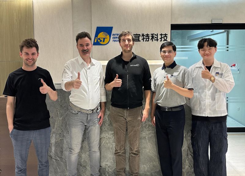
PRESS RELEASE — QuantumDiamonds GmbH, the Munich-based pioneer in quantum sensing-based semiconductor testing, today announced the successful deployment of its QDm.1 system at Integrated Service Technology (iST) in Hsinchu, Taiwan. Following the company’s expansion into Asia in March and successful installation of the system in the US, the deployment marks QuantumDiamonds’ first installation in Asia and a landmark moment for the adoption of quantum sensing technology in high-volume semiconductor failure analysis.
Across Asia’s fast-expanding semiconductor landscape, yield loss remains one of the industry’s most costly obstacles – stalling innovation, inflating production costs, and deepening the memory chip shortage driven by surging AI demand. QuantumDiamonds’ non-destructive failure analysis technology addresses this challenge head-on, giving manufacturers the actionable intelligence needed to eliminate failed chips and optimize their production workflows for greater efficiency and output.
“Completing our first Asia installation at iST is a defining moment for QuantumDiamonds,” said Peter Lemmens, Managing Director APAC at QuantumDiamonds. “Hsinchu is home to some of the most sophisticated chip manufacturing and testing operations in the world. Being embedded here, in partnership with a laboratory of iST’s caliber, gives us an outstanding platform to demonstrate what quantum sensing can deliver – and to build from.”
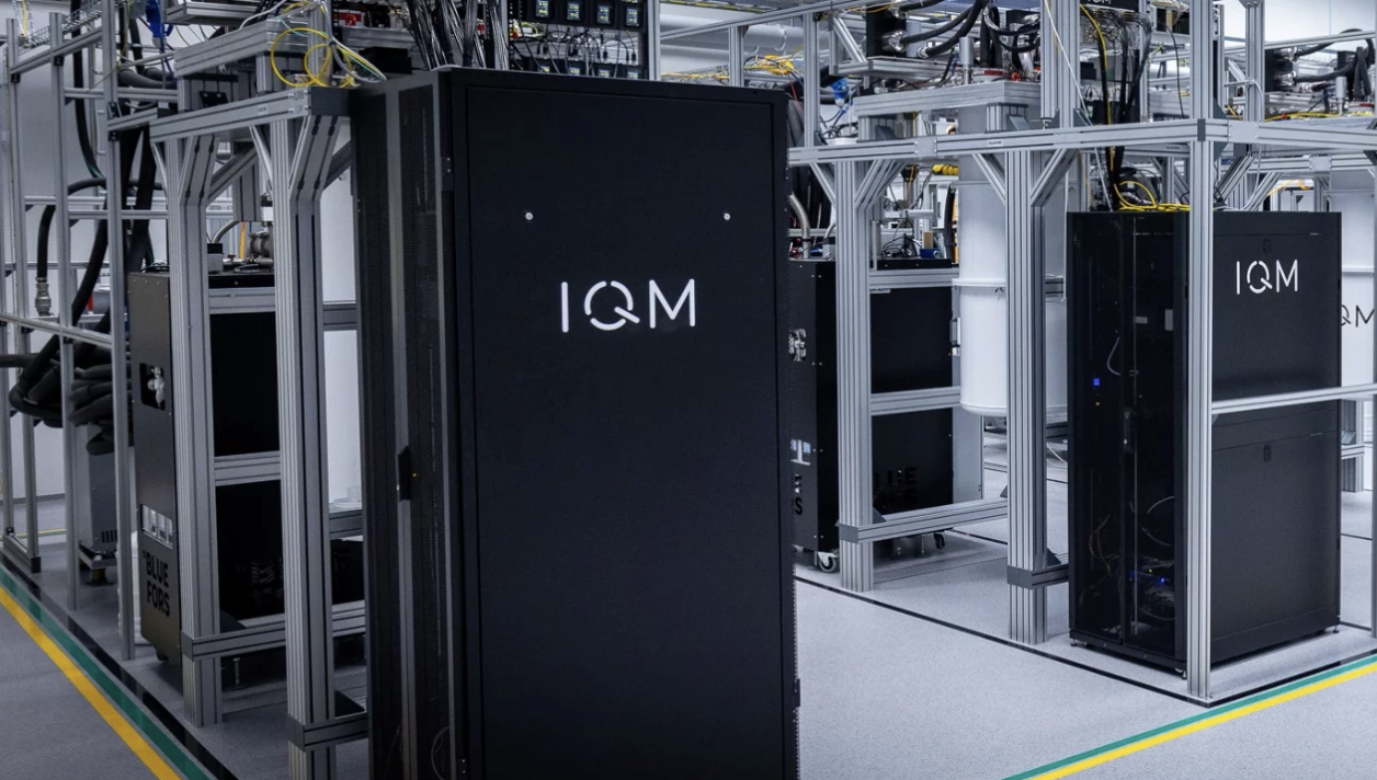
QuantumDiamonds has commercialized the world’s first integrated quantum sensing system for semiconductor failure analysis. Its QDm.1 system based on patented Quantum Diamond Microscopy (QDM) technology delivers non-destructive, high-resolution 3D imaging of current pathways in advanced chip architectures, including 2.5D and 3D packages, backside power networks, and wide bandgap materials such as GaN and SiC.
iST, one of Asia’s leading independent semiconductor testing and failure analysis laboratories, selected the QDm.1 to strengthen its failure analysis capabilities for customers operating at advanced technology nodes and in advanced packaging architectures. The system is now fully operational at iST’s Hsinchu facility, located at the heart of Taiwan’s world-renowned semiconductor cluster.
“Taiwan is the epicenter of advanced semiconductor manufacturing, and iST is one of the most respected failure analysis laboratories in the region,” said Kevin Berghoff, CEO of QuantumDiamonds. “This installation is more than a commercial milestone – it is validation that quantum sensing is ready for the most demanding real-world environments in the industry. We are proud to partner with iST and look forward to supporting their customers with a capability that simply did not exist before.”
“Our customers are working at the leading edge of chip complexity, and they need failure analysis tools that can keep pace,” said Dr. Sean Shen, Director of Failure Analysis Engineering Division at iST. “The QDm.1 gives our engineers a fundamentally new way to interrogate advanced devices – non-destructively, in three dimensions, and at a speed that fits our workflow. We see significant potential for this technology across the range of advanced packaging and high-density interconnect challenges our customers face.”
The installation at iST follows strong and growing demand across the Taiwan, Japan, and Korea semiconductor ecosystems, where nine of the world’s top ten chipmakers are already engaged with QuantumDiamonds.