
Insider Brief
- QuantaMap and Leiden University have demonstrated a new multi-modal microscope that enables simultaneous nanoscale imaging of heat, magnetism, structure and electrical behavior on operational quantum chips, with results published in Nano Letters.
- The platform moves quantum chip characterization from idealized lab conditions to real devices, allowing researchers to correlate intertwined physical properties in a single scan without disturbing the sample.
- The technology is designed to enable nanoscale root-cause analysis during fabrication, improve yield and design feedback loops, and is now being commercialized for quantum materials research and chip manufacturing.
PRESS RELEASE — Dutch quantum technology startup QuantaMap and Leiden University have demonstrated a new class of microscope for quantum chip inspection. It enables simultaneous nanoscale imaging of heat, magnetism, structure, and electrical behavior.
As quantum technologies transition from laboratory demonstrations to engineered systems, understanding how quantum chips behave locally inside end-user devices has become a critical bottleneck.
This new research by QuantaMap and Leiden University, published in Nano Letters (read it here: https://pubs.acs.org/doi/10.1021/acs.nanolett.5c04571), introduces the microscope as a multi-modal imaging platform that moves quantum characterization out of idealized test conditions and onto actual quantum chips. It is here where performance, yield, and reliability are ultimately determined.
A Single Scan Reveals Everything
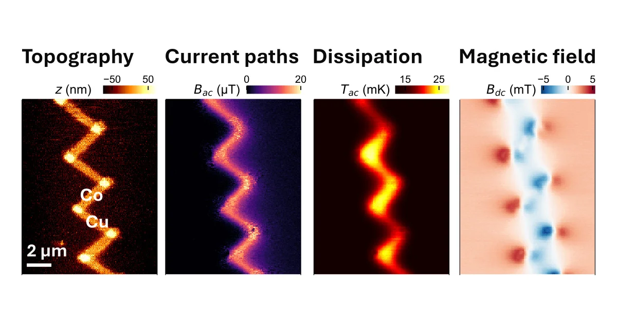
The microscope enables research teams to probe multiple interacting physical phenomena at once, with nanoscale resolution and without disturbing the chip under test.
“In a real quantum device, all physical properties are closely intertwined. If you only study one aspect at a time, you never get ahead. With our microscope, we reveal the relationships between non-equilibrium properties such as current and dissipation, and how those relate to chip structure,” explains lead author Matthijs Rog of Leiden University.
“This is groundbreaking for our research into the intricate workings of quantum materials.”
This multimodal imaging is performed extremely close to the sample surface using tapping mode feedback allowing for stability during extended measurement campaigns and imaging of realistic, nanostructured devices — including operational quantum chips and exotic quantum materials.
Why this Matters for the Quantum Industry
“Current chip testing relies mainly on electrical characterization of fully finished chips inside quantum computers – a process that takes weeks per chip and if the performance of some qubits is reduced, it cannot reveal the underlying reason,” says Johannes Jobst, founder and CEO of QuantaMap.
“This new imaging platform addresses that gap. The ability to perform root‑cause analysis at the nanoscale makes it possible to identify reasons for failure in quantum chips at any fabrication stage, correlating device performance with local material behavior, and faster design–fabrication–test feedback loops.”
As a result of this new technology, fab yield and consistency can be increased, accelerating design optimization and the transition toward scalable quantum manufacturing.
A New Product for the Quantum Market
QuantaMap is now working to bring these microscope systems to the market for quantum materials research and quantum chip manufacturing.