Insider Brief
- Scientists have demonstrated superconductivity in heavily gallium-doped germanium, achieving zero resistance at 3.5 Kelvin under controlled growth conditions.
- The team used molecular beam epitaxy to precisely integrate gallium atoms into the germanium lattice, stabilizing the crystal despite high doping levels.
- The material’s compatibility with existing semiconductor platforms opens pathways for scalable quantum circuits, sensors, and low-power cryogenic electronics.
PRESS RELEASE — According to the NYU — Scientists have long sought to make semiconductors – vital components in computer chips and solar cells—that are also superconducting, thereby enhancing their speed and energy efficiency and enabling new quantum technologies. However, achieving superconductivity in semiconductor materials such as silicon and germanium has proved challenging due to difficulty in maintaining an optimal atomic structure with the desired conduction behavior.
In a newly published paper in the journal Nature Nanotechnology, an international team of scientists reports producing a form of germanium that is superconducting—able to conduct electricity with zero resistance, which allows currents to flow indefinitely without energy loss, resulting in greater operational speed that requires less energy.
“Establishing superconductivity in germanium, which is already widely used in computer chips and fiber optics, can potentially revolutionize scores of consumer products and industrial technologies,” says New York University physicist Javad Shabani, director of NYU’s Center of Quantum Information Physics and the university’s newly established Quantum Institute, one of the paper’s authors.
“These materials could underpin future quantum circuits, sensors, and low-power cryogenic electronics, all of which need clean interfaces between superconducting and semiconducting regions,” adds Peter Jacobson, a physicist at the University of Queensland and one of the paper’s authors. “Germanium is already a workhorse material for advanced semiconductor technologies, so by showing it can also become superconducting under controlled growth conditions there’s now potential for scalable, foundry-ready quantum devices.”
Semiconductor materials such as germanium and silicon, both diamond-like crystals, are group IV elements, whose electronic behavior straddles that of metals and insulators. These materials are useful in manufacturing because of their flexibility and durability. Achieving superconductivity in these elements is accomplished by manipulating their structure to introduce numerous conducting electrons. These electrons interact with the germanium crystal to pair with one another and move without resistance — a process that has historically been challenging to control at the atomic level.
“Establishing superconductivity in germanium, which is already widely used in computer chips and fiber optics, can potentially revolutionize scores of consumer products and industrial technologies.” New York University’s Javad Shabani, director of NYU’s Center of Quantum Information Physics and Quantum Institute
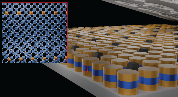
In the Nature Nanotechnology work, the scientists created germanium films that were heavily infused with a softer element, gallium, which is also commonly used in electronics. This long-established process, known generically as ‘doping,’ alters a semiconductor’s electrical properties—but at high levels of gallium, typically the material becomes unstable, leading to a breakdown of the crystal and no superconductivity.

However, in the newly reported results, the scientists, using advanced X-ray techniques, demonstrate a new technique, which forces gallium atoms to replace germanium atoms within the crystal at higher-than-normal levels. This process slightly deforms the shape of the crystal, but nonetheless keeps a stable structure that can conduct electricity with zero resistance at 3.5 Kelvin – or approximately -453 degrees Fahrenheit—thereby becoming superconducting.
“Rather than ion implantation, molecular beam epitaxy was used to precisely incorporate gallium atoms into the germanium’s crystal lattice,” notes Julian Steele, a physicist at the University of Queensland and one of the paper’s authors. “Using epitaxy—growing thin crystal layers—means we can finally achieve the structural precision needed to understand and control how superconductivity emerges in these materials.”

“This works because group IV elements don’t naturally superconduct under normal conditions, but modifying their crystal structure enables the formation of electron pairings that allow superconductivity,” observes Shabani.
The research, which also included researchers from ETH Zurich and the Ohio State University, was supported, in part, by the US Air Force’s Office of Scientific Research (FA9550-21-1-0338).
Source — NYU


