Caltech Researchers Extend Optical Fiber’s Ultralow Loss Performance to Photonic Chips


Insider Brief
- California Institute of Technology researchers have demonstrated fiber-like ultralow optical loss on silicon wafers at visible wavelengths, enabling a new class of highly efficient and coherent photonic integrated circuits.
- The team fabricated germano-silicate waveguides using standard semiconductor lithography and surface reflow techniques, achieving up to a 20-fold loss improvement over silicon nitride at visible wavelengths and more than 100-fold gains in laser coherence.
- The approach extends chip-scale photonics across violet to near-infrared bands, with applications spanning optical clocks, atomic sensors, data-center communications, and future quantum and precision-measurement systems, as reported in a recent paper in Nature.
- Image: Hao-Jing Chen
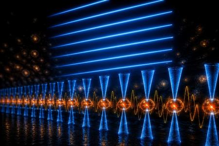
PRESS RELEASE — Caltech scientists have developed a way to guide light on silicon wafers with low signal loss approaching that of optical fiber at visible wavelengths. This accomplishment paves the way for a new generation of ultra-coherent and efficient photonic integrated circuits (PICs), which will have a profound impact in a variety of on-chip applications including precision measurements, such as optical clocks for timing and gyroscopes for rotation as well as AI data-center communications and even quantum computing.
Even if we are largely unaware of it, optical fiber is all around us. It is what connects our digital world, enabling us to communicate and share data nearly instantaneously regardless of distance. Optical fiber can do this, in large part, because it is made from extremely pure glass and is carefully engineered to be ultrasmooth; when light enters at one end of a fiber, nearly the entire signal continues to the other end without being absorbed, scattered, or otherwise lost. This is what researchers describe as ultralow-loss performance.
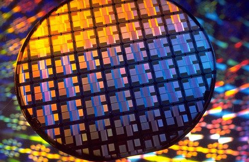
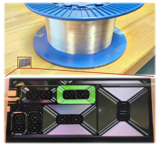
“For years, we have been working to translate the spool-based fabrication of optical fiber onto silicon wafers, while trying to preserve the fiber’s hallmark of ultralow loss,” says Kerry Vahala (BS ’80, PhD ’85), the Ted and Ginger Jenkins Professor of Information Science and Technology and Applied Physics at Caltech. “We have developed a method to print optical circuits, made from the same material as optical fiber, directly onto the same 8- and 12-inch wafers used for computer chips. This shift toward fiber-like performance, especially in the visible bands, will enable new technologies that benefit from negligibly low circuit energy loss.”

The scientists describe their method in a paper recently published in the journal Nature. The lead authors of the paper are Caltech postdoctoral scholar Hao-Jing Chen and graduate student Kellan Colburn (MS ’25), who completed the work in Vahala’s lab.
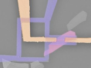
To make its waveguides (nanoscale on-chip pathways that channel light), the team adapts germano-silicate, the same glass material used in optical fiber, through a lithography-based manufacturing process. The waveguides are laid out in a spiral geometry to extend their optical path length, analogous to winding light around a fiber spool but with a significantly smaller footprint enabled by nanofabrication. “Germano-silicate waveguides demonstrate extremely low loss and are also readily adaptable to efficiently transfer light between optical fibers and semiconductor lasers, which is of paramount importance in reducing the overall energy cost of server infrastructure,” says Henry Blauvelt (PhD ’83), a visiting associate in applied physics and material science at Caltech; chief technology officer at Emcore, a company specializing in photonic circuits; and an author of the recent paper.
Devices made with the Caltech team’s new platform have already matched, at near-infrared wavelengths, previous top-performing devices made from silicon nitride, a material widely used in optics because of its low-loss performance for transmitting data. Importantly, the new material significantly outperforms silicon nitride at visible wavelengths. “Due to the comparatively low melting temperature of the material, we can put our devices into a furnace to ‘reflow’ the surface of our waveguides to get their smoothness down to the level of individual atoms, which largely suppresses the severe scattering loss that has limited conventional visible PICs,” Chen says. “At visible wavelengths, our recent platform exceeds silicon nitride’s record by a factor of 20, and we have more room to improve.”
Loss dramatically impacts optical device performance. For example, laser devices fabricated using the new platform exhibit more than a 100-fold improvement relative to predecessors in terms of how long light remains coherent.
“The expanded wavelength coverage our method offers will support many important atomic operations, making chip-scale atomic sensors, optical clocks, and ion-trap systems possible,” Chen says.
Colburn acknowledges that it might at first seem “a little ridiculous” that the researchers are aiming for losses that can be described by percentages over kilometers. “After all, our chips are only 2 centimeters across. But, in reality, there are a lot of applications where this would be very powerful,” he says. For example, think of the ring resonator, a fundamental optical device widely used in both fundamental science and data transmission. In ring resonators, light enters at one point and gets fed into a ring where it continues to propagate for a long time, a process that resonantly enhances the light at a few frequencies. Even though the ring is just millimeters in scale, the effective path that light traces in such a resonator is determined by the loss of the waveguides. “That’s where low loss over meters, or ultimately kilometers, really matters,” Colburn says. “The longer light can circulate, the higher the performance of resulting devices can be.” For lasers that use these resonators to improve coherence, every factor of 10 reduction in loss translates to a factor of 100 improvement in coherence.
More generally, the ability to engineer ultralow-loss waveguides in the visible bands has many applications. “One of the reasons this is so compelling is that it has a Swiss Army–knife quality—it can be applied in a wide range of settings,” Vahala says. To illustrate this point, the Caltech team describes in the paper several optical devices they built with the new material. This includes ring resonators, different types of lasers, and nonlinear resonators that generate a range of frequencies.
And the team is just getting started, Vahala says. “We haven’t gone as far as we want to go, but we’ve made significant progress over the last five years, and that’s what we’re reporting on here,” he says.
The paper is titled “Towards fibre-like loss for photonic integration from violet to near-infrared”: https://www.nature.com/articles/s41586-025-09889-w. Additional Caltech authors are graduate students Peng Liu (MS ’24), Hongrui Yan, Jinhao Ge (MS ’24), Jin-Yu Liu (MS ’24), and Phineas Lehan; former graduate student Qing-Xin Ji (PhD ’25); former postdoctoral scholar Zhiquan Yuan (PhD ’24); and Hanfei Hou who participated in the research as part of the Summer Undergraduate Research Fellowship program. Dirk Bouwmeester of UC Santa Barbara and Leiden University in the Netherlands and Christopher Holmes and James Gates of the University of Southampton in the United Kingdom are also authors. The work was funded by grants from the Defense Advanced Research Projects Agency, the Air Force Research Laboratory, the Engineering and Physical Sciences Research Council, and the Kavli Nanoscience Institute at Caltech.

Keep track of everything going on in the Quantum Technology Market. In one place.

Matt Swayne
With a several-decades long background in journalism and communications, Matt Swayne has worked as a science communicator for an R1 university for more than 12 years, specializing in translating high tech and deep tech for the general audience. He has served as a writer, editor and analyst at The Quantum Insider since its inception. In addition to his service as a science communicator, Matt also develops courses to improve the media and communications skills of scientists and has taught courses.
[email protected]

Stay Ahead of Quantum
Get the latest research, company news, and market intelligence every week.
MENTIONED IN THE ARTICLE

California Institute of Technology
The California Institute of Technology, situated in Pasadena, California, is a private research university. It has played a crucial role in numerous contemporary scientific breakthroughs and stands alongside a select few technology institutes in the United States that prioritize teaching in pure and applied sciences.
→

UC Santa Barbara
The University of California, Santa Barbara, is a public research university located in Santa Barbara, California, United States. It operates within the University of California system. Originating from an independent teachers' college in 1891, UCSB became part of the California State system in the 1920s and later joined the University of California system in 1944. It holds the distinction of being the third-oldest undergraduate campus within the system, following UC Berkeley and UCLA.
→

University of Southampton
The University of Southampton is a public research university located in Southampton, England. As a founding member of the Russell Group, a collection of research-intensive UK universities, Southampton holds a position among the top 100 universities globally. Its history dates back to 1862 when it was established as the Hartley Institution. Later, in 1952, Queen Elizabeth II granted the university a royal charter, marking one of her initial official actions as monarch.
→

Defense Advanced Research Projects Agency (DARPA)
The Defense Advanced Research Projects Agency (DARPA) is an independent research and development agency within the U.S. Department of Defense (DoD) established in 1958 to prevent and create strategic technological surprises for national security. Operating with a relatively small staff of program managers who are empowered to take high-risk, high-reward approaches, DARPA functions by funding cutting-edge research in academia, industry, and government laboratories rather than conducting research in-house. Its mission focuses on creating revolutionary technologies—such as the Internet (ARPANET), stealth technology, GPS, and mRNA vaccine platforms—that transition into practical military and civilian applications. DARPA programs are typically finite in duration and demand transformational breakthroughs rather than incremental improvements, positioning the U.S. at the forefront of technological innovation.
→

Air Force Research Laboratory Quantum Group
The Air Force Research Laboratory is partnering with industry, academia, and the Department of Defense to apply quantum information science to Air Force concerns. AFRL has formally joined the IBM Q Network, the first ever partnership of its kind in the Department of Defense. This alliance will provide AFRL and its collaborators with access to commercial quantum systems to explore practical applications relevant to the Air Force. Early applications include optimization problems, speed-up of machine learning algorithms and quantum chemistry simulation. The Extreme Computing facility by the Air Force Research Laboratory (AFRL), is now open in New York. It is involved in quantum computing research, ranging from development, integration and deployment of advanced computing technologies for the Department of the Air Force. The AFRL Information Directorate received funding for five major projects. They include: 1. $10 million for Distributed Quantum Networking Testbed and Quantum Cloud Computing Environment, 2. $4 million for Photonic Quantum Computing, which will develop a next-generation ion trap computer. 3. $10 million for Enhancements and Operational Readiness improvements for Trusted DoD/Federal Unmanned Aircraft Systems. This system will manage UAS traffic to support the emerging Federal Aviation Administration/National Aeronautics and Space Administration Advanced Air Mobility vision and provide a real-time interface to Air Traffic Control. 4. $10 million for a Joint All-Domain Command and Control testbed which creates an operational-like environment that allows the warfighter to test cutting-edge technology and tools and provide feedback for researchers. 5. $10 million for a Multi-Domain Radio Frequency Spectrum Test environment. Total government funding involved in the AFRL currently amounts to ~$44 million USD.
→