Insider Brief
- D-Wave Quantum Inc. demonstrated scalable on-chip cryogenic qubit control for gate-model quantum computing, reducing wiring requirements while preserving qubit fidelity and addressing a key barrier to commercial-scale systems.
- The company showed that its multiplexed control technology, already used in annealing quantum processors to manage tens of thousands of qubits with limited wiring, can be applied to gate-model architectures to enable larger, more practical processors.
- The result was achieved using a multichip superconducting package that integrates high-coherence fluxonium qubits with cryogenic control electronics, leveraging established fabrication methods and contributions from NASA’s Jet Propulsion Laboratory.
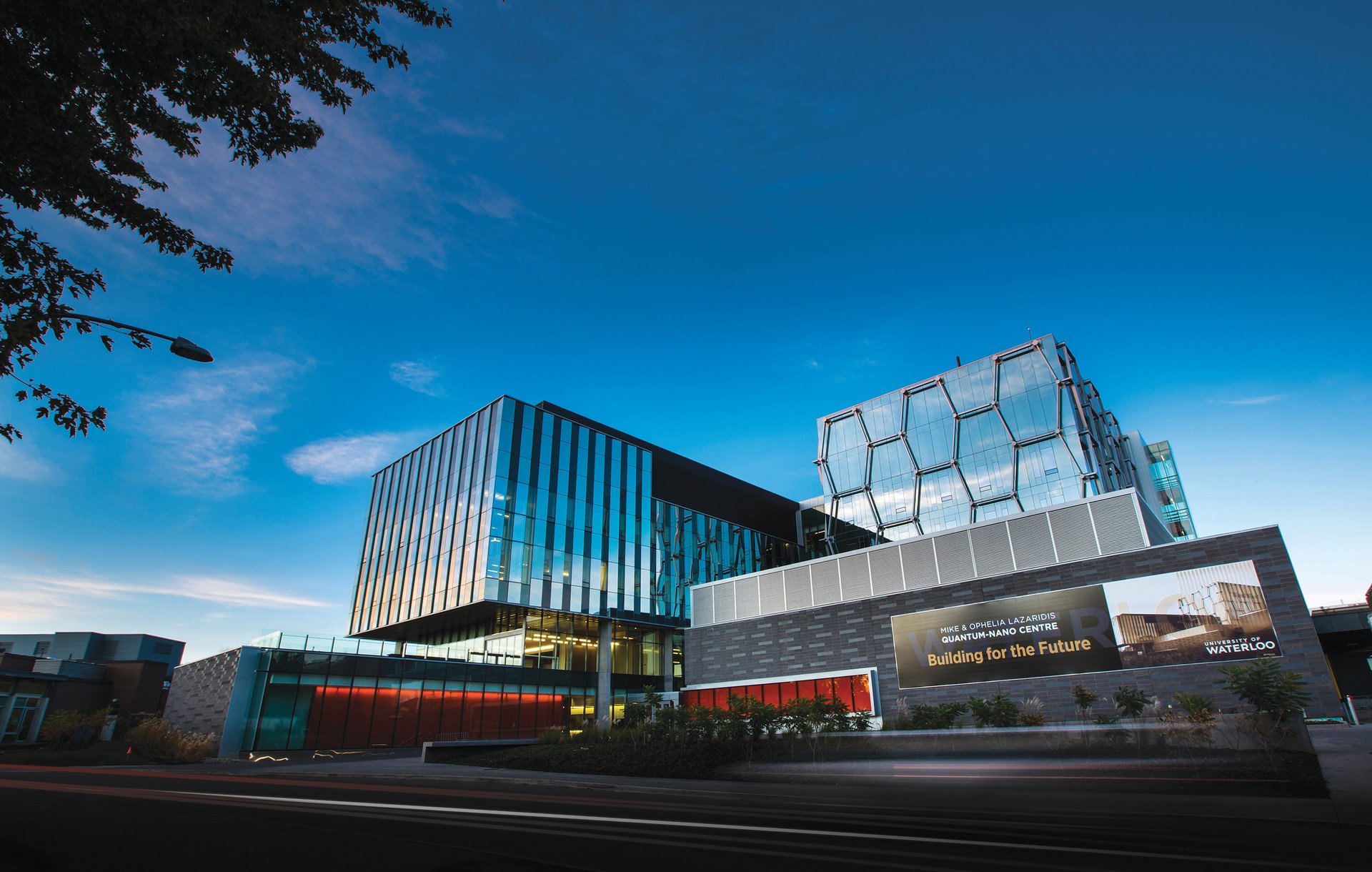
PRESS RELEASE — D-Wave Quantum Inc. (NYSE: QBTS) (“D-Wave” or the “Company”), a leader in quantum computing systems, software, and services, and the world’s first commercial supplier of quantum computers, today announced a breakthrough in gate-model quantum computing with the successful demonstration of scalable on-chip cryogenic control of qubits. This industry-first milestone advances the development of commercially viable gate-model quantum computers by significantly reducing the wiring required to control large numbers of qubits without degrading qubit fidelity.
This achievement validates that the on-chip cryogenic control technology D-Wave developed for its commercial annealing quantum processing units (QPUs) can also be applied to its gate-model architectures. In D-WaveTM annealing systems, the control technology uses multiplexed digital-to-analog converters to control tens of thousands of qubits and couplers with just 200 bias wires. The same control technology can also reduce gate-model wiring complexity while maintaining qubit fidelity, enabling large-scale, practical gate-model QPUs.
“Without on-chip control and multiplexing, useful gate-model quantum computers require an impractically large amount of wiring and massive cryogenic enclosures,” said Dr. Trevor Lanting, chief development officer at D-Wave. “Scalability is fundamental to the growth and increasing adoption of this technology, and controlling more qubits with less wiring enables us to build larger processors with a smaller footprint. We believe this historic milestone positions D-Wave to deliver the industry’s first truly scalable, commercial-grade gate-model system.”
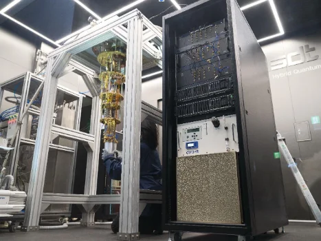
Using superconducting bump bonding and advanced cryogenic packaging techniques, D-Wave built a multichip package that integrates a high-coherence fluxonium qubit chip with a multilayer control chip. Key components of the multichip package were fabricated leveraging deep expertise and processes at the NASA Jet Propulsion Laboratory, a research and development lab federally funded by NASA and managed by Caltech.
D-Wave’s superconducting technology builds on decades of established micro-circuit manufacturing techniques, enabling faster, lower-cost scaling using proven supply chains. Superconducting qubits can execute gates significantly faster than trapped ions, neutral atoms, or photonics—a gap that matters as systems scale and fidelity improves. With more than 20 years of pioneering work in superconducting quantum computing, and over 60 percent of the company’s patents spanning both annealing and gate-model technologies, D-Wave is uniquely positioned to develop foundational technologies across the full quantum landscape.
To learn more about D-Wave’s latest product roadmap and progress across annealing and gate-model quantum computing, hybrid-quantum solvers and quantum-AI, join us at Qubits 2026, January 27 and 28, 2026, in Boca Raton, Florida. To register for Qubits 2026 visit: https://www.qubits.com.