
Insider Brief
- China has introduced a photonic quantum chip reported to accelerate complex calculations by more than a thousandfold, marking one of its most significant advances in next-generation computing, according to the South China Morning Post.
- The chip, developed by CHIPX and Turing Quantum, features dense optical integration, rapid design cycles, and a pilot production line capable of producing 12,000 six-inch wafers annually, positioning China to scale photonic hardware for data centers, AI workloads and quantum research.
- Despite the progress, key uncertainties remain around performance stability, error behavior and mainstream deployability, and claims of 1,000-fold gains over leading GPUs depend heavily on specific tasks rather than general-purpose computing.
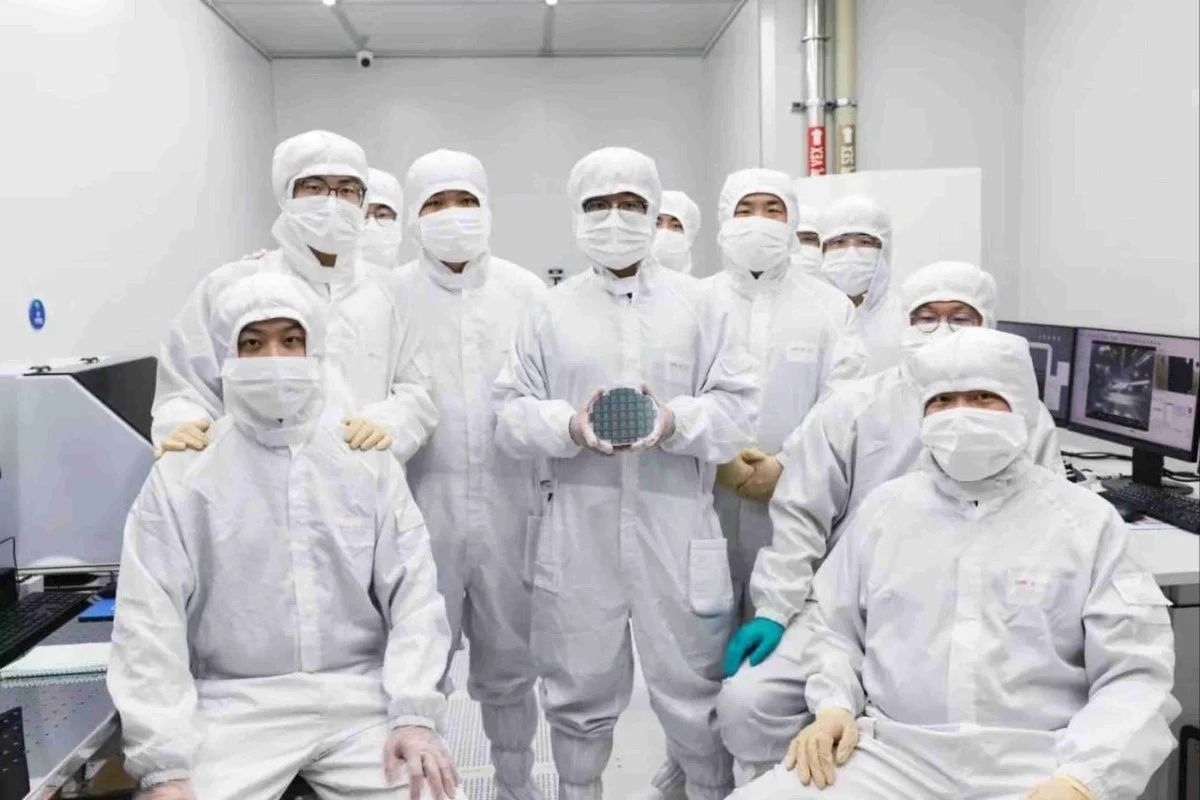
- Image: Researchers at CHIPX pose for a photo with their high-performance 6-inch thin-film lithium niobate chip, an advance that is poised to accelerate progress in AI and quantum computing. (Handout, SCMP)
What Is China’s New Photonic Quantum Chip and Why Does It Matter?
China has unveiled a photonic quantum chip that marks one of the country’s largest single leaps in computing power, according to reporting from the South China Morning Post (SCMP). The new chip, developed by a university-affiliated research institute and a Shanghai start-up, is reportedly designed to speed up complex calculations by more than a thousandfold.
The chip was one of 17 technologies recognized at the 2025 World Internet Conference Wuzhen Summit and was described by its developers as delivering performance beyond the limits of classical machines. Photonic quantum chips use light instead of electricity to process information. Because light moves faster and carries more data while using less energy, these chips are seen as a promising bridge between today’s computers and fully quantum systems still under development.
“Achieving co-packaging technology for photons and electronics, chip-level integration and wafer-scale mass production of photonic quantum chips – I believe this is a world first,” Jin Xianmin, a physics professor at the university and founder of Turing Quantum, told SCMP. “We anticipate developing chips capable of handling larger numbers of photons in the near future,” he told mainland media on the day of the awards ceremony.

China’s new device is already being deployed across aerospace, biomedicine and financial modeling, according to the newspaper. Developers see it as a step toward hybrid architectures that mix classical and quantum-like components to tackle heavy workloads such as molecular simulation, materials design, risk analysis and large-scale optimization.
Use Cases for China’s Photonic Chip:
| Industry | Application | Benefit |
|---|---|---|
| Aerospace | Simulation and modeling | Faster analysis and reduced computational cost |
| Biomedicine | Molecular and protein modeling | Better predictive outcomes and discovery speed |
| Finance | Risk modeling and optimization | Faster large scale Monte Carlo type analysis |
| AI workloads | Data center acceleration | Higher bandwidth and lower energy demand |
What Makes China’s Photonic Quantum Platform Different?
The chip is the result of work by the Chip Hub for Integrated Photonics Xplore, or CHIPX, an institute in Wuxi connected to Shanghai Jiao Tong University, and Turing Quantum, a photonics start-up based in Shanghai. As reported by the newspaper, the university said that CHIPX has completed a full production loop for photonic chips, including design, wafer fabrication, packaging, testing and system integration. That means the institute can design and manufacture entire chip systems in-house, a capability that is rare even among global firms working with advanced photonics.
Photonic integrated circuits operate by manipulating photons using structures that control light’s colour, timing and distribution. Because these degrees of freedom can be combined, a single chip can handle many channels of information at once.
China’s new device is unusually dense, packing more than 1,000 optical components onto a six-inch silicon wafer. Researchers call this level of monolithic integration world-class, according to the Post.
The chips also feature high-performance data transmission and large bandwidth. Their architecture is designed with enough flexibility to scale toward systems that could someday support a million qubits — an ambition shared across quantum hardware companies globally. Although true quantum processors with millions of qubits are still years away, developers are using photonic chips to prototype algorithms, model quantum behavior and accelerate classical computation that supports quantum research.
| Feature | What It Means | Why It Matters |
|---|---|---|
| Full in house production loop | Full in-house production loop | Enables faster iteration and reduces bottlenecks |
| Over one thousand optical components | CHIPX controls design, fabrication, packaging, and testing | Supports many parallel information channels |
| Thin film lithium niobate | Material that enables very low optical loss | Improves signal fidelity and stability |
| Large bandwidth architecture | Design that can handle many simultaneous operations | High optical density on a six-inch wafer |
How Much Faster Can China Build and Iterate These Chips?
Beyond raw performance, the platform also reportedly shortens development timelines more in line with commercial production. The SCMP reported that design cycles that previously took six months can now be completed in as little as two weeks. That ability to iterate quickly is critical in photonics, where even slight adjustments in geometry can significantly change how light moves through the system.
Photonic chips have long been known to offer advantages in speed and energy efficiency, but manufacturing them has been difficult. The materials often require precise handling, and defects at the nanoscale can compromise performance. A major challenge has been finding ways to build them at scale, using production lines similar to those used for traditional semiconductor wafers.
CHIPX has begun addressing that bottleneck. In June, the institute launched China’s first pilot production line for six-inch thin-film lithium niobate photonic wafers, according to the newspaper. Lithium niobate is a material valued for its ability to modulate and guide light with very low loss.
The new line can manufacture about 12,000 wafers a year, with each providing roughly 350 chips.
A capacity of 12,000 six-inch photonic wafers per year is modest compared with mature semiconductor fabs, which produce hundreds of thousands of wafers annually at 200mm or 300mm scales. But in the photonics sector — especially for thin-film lithium niobate — this level of output represents a meaningful industrial foothold.
How Close Is China to Commercial Deployment of These Chips?
The institute aims to increase yields, explore new materials and eventually upgrade to eight-inch wafers.
Larger wafers would allow more chips to be produced at once, lowering costs and enabling wider industrial deployment. According to SCMP, CHIPX is encouraging collaboration with companies across 5G, 6G, cloud computing, artificial intelligence data centers and quantum networking, areas where photonic chips could solve bottlenecks in bandwidth and energy consumption.
The announcement comes at a time when the global race in photonic computing is intensifying.
The Post reported that in February, California-based PsiQuantum announced plans to use 300-millimetre wafer manufacturing for its silicon photonics line, a scale similar to that used in leading-edge semiconductor fabs. Europe is also investing in photonics as part of its broader quantum-technology programs.
What Unknowns Still Limit China’s Photonic Quantum Chip?
Taking a step back, claims that the device can outstrip leading NVIDIA graphics processors by a factor of 1,000 reflect the type of performance gains quantum approaches are expected to deliver on certain classes of problems, though these comparisons are often faulty, as they depend heavily on the underlying task and are not equivalent to general-purpose speed.
Quantum hardware, theoretically, can solve specific equations at rates that classical machines cannot match, but turning that theoretical edge into reliable, deployable systems remains an industry-wide challenge.
Despite fast progress, key questions remain about scaling limits, uniformity, stability and behavior under real world workloads that differ from controlled laboratory conditions.
Public disclosures have focused on fabrication capacity, packaging and optical density, but far less is known about error behavior, device uniformity, long-term stability, and how well the chips perform across a wide range of workloads outside controlled test environments.
Photonic systems are sensitive to manufacturing imperfections and thermal drift, and it is unclear how much additional engineering will be required before the technology becomes truly mainstream in data centers or high-performance computing sites.
Frequently Asked Questions
What is China’s new photonic quantum chip?
China has unveiled a photonic quantum chip developed by CHIPX (Chip Hub for Integrated Photonics Xplore) and Turing Quantum that reportedly accelerates complex calculations by more than a thousandfold. The chip uses light instead of electricity to process information and was recognized at the 2025 World Internet Conference Wuzhen Summit.
Who developed this chip?
The chip was jointly developed by CHIPX, a Wuxi-based institute affiliated with Shanghai Jiao Tong University, and Turing Quantum, a hi-tech start-up in Shanghai.
How does photonic computing work?
Photonic chips use light (photons) instead of electricity to process information. Because light moves faster and carries more data while using less energy, these chips offer advantages in speed and energy efficiency over traditional electronic processors.
What makes China’s chip different from other photonic chips?
China’s device packs more than 1,000 optical components onto a six-inch silicon wafer. CHIPX has completed a full production loop for photonic chips, including design, wafer fabrication, packaging, testing and system integration, allowing them to design and manufacture entire chip systems in-house.
How fast can China produce these chips?
Design cycles that previously took six months can now be completed in as little as two weeks. CHIPX launched China’s first pilot production line for six-inch thin-film lithium niobate photonic wafers in June, capable of manufacturing about 12,000 wafers a year, with each wafer providing roughly 350 chips.
Where is this chip already being used?
China’s new device is already being deployed across aerospace, biomedicine and financial modeling. Developers see it as a step toward hybrid architectures that tackle heavy workloads such as molecular simulation, materials design, risk analysis and large-scale optimization.
Is this actually a quantum computer?
The chip performs classical optical computing using bright light, not quantum computing. It doesn’t use single-photon sources, entanglement, cluster states, quantum gates, or any features that make a device meaningfully quantum. The chip accomplishes its performance by exploiting the natural parallelism of light interference, not by harnessing quantum superposition or entanglement.
What are China’s plans for this technology in the future?
The institute aims to increase yields, explore new materials and eventually upgrade to eight-inch wafers. Larger wafers would allow more chips to be produced at once, lowering costs and enabling wider industrial deployment. The architecture is designed with enough flexibility to scale toward systems that could someday support a million qubits.