Insider Brief
- Russian researchers have developed a sub-ångström fabrication technology enabling scalable production of superconducting quantum processors with thousands of qubits.
- The iDEA method, using ion beam-induced defect activation, achieves ±0.2 Å precision in tunnel dielectric thickness, improving qubit uniformity and reducing operational errors.
- The technique outperforms existing methods in speed and precision, and has been validated in quantum coprocessors, with potential applications across other post-CMOS architectures.
Editor’s Note: The following is computer translated version of a news release issued in Russian. Apologies for any mis-translations of terms or terminology.
PRESS RELEASE — The nanotechnology center of the Quantum Park cluster at Bauman Moscow State Technical University (BMSTU), in collaboration with the Federal State Unitary Enterprise “Dukhov Automatics Research Institute” (VNIIA), has announced the development of a sub-ångström fabrication technology for next-generation processors.
The researchers have discovered a method and developed a technique to create logic elements for computing devices using new physical principles with a precision of ±0.2 ångströms (1 Å = 0.1 nanometers ≈ the diameter of an atom). This iDEA technology enables the mass production in Russia of quantum processors with thousands of superconducting qubits (artificial atoms), each manufactured to exact specifications, accelerating progress toward practical hybrid supercomputers.

Russian Quantum Center (RQC) scientific director Alexey Akimov, said: “Researchers from Bauman Moscow State Technical University have proposed a new method to solve an important problem: adjusting already manufactured qubits with a focused beam of neon ions. The problem is that “artificial atoms,” or qubits made of superconducting materials, differ significantly after manufacturing, which makes operation of a quantum computer extremely difficult. Currently, this problem is partially addressed by creating additional elements on the chip — control qubits. The Russian researchers approached the matter differently, trying to find a method to adjust qubits “in hardware.” They succeeded, and the qubits’ properties are preserved for a long time; that is, the corrected qubits remain the same. Google apparently uses similar correction methods, but this is the first method of adjusting qubits in hardware in Russia. This is critically important for the successful development of quantum computers based on a superconducting platform. This platform remains the main one for large IT companies investing in quantum technologies.”
The results have been published in Science Advances, and the technology is patented in Russia with international patent filings underway.
Sub-Ångström Precision: Why It Matters
Modern processors for supercomputing, graphics, and AI contain tens or even hundreds of billions of transistors on a single silicon chip. Shrinking transistor size to the scale of atoms is a major goal in the semiconductor industry. However, only a few companies are entering the “ångström era” of CMOS technologies. Intel introduced 18Å (1.8 nm) technology in 2025, Samsung is preparing 12Å (1.2 nm) SF2, and TSMC is developing 20Å (2 nm) N2 nodes.
These technologies typically achieve transistor dimensions of 12–14 nm, with critical attention on gate dielectric thickness, often between 1.5–2 nm. Leading manufacturers have achieved dielectric thickness control with ±0.2 nm (±2 Å) precision.
Further miniaturization demands new physical principles of operation. Hybrid computing systems that integrate current CMOS platforms with post-CMOS coprocessors could offer vast performance gains. Such systems have the potential to transform sectors ranging from healthcare and transportation to space exploration.
Superconducting quantum coprocessors are currently the leading post-CMOS platform. Countries including the U.S., China, Japan, and EU members are pursuing hybrid information processing systems based on superconducting qubits—artificial atoms manufactured on silicon chips using methods similar to traditional CMOS. But quantum systems require far greater fabrication precision: artificial atoms must be nearly identical, matching the uniformity of natural atoms.
iDEA Technology: Sub-Ångström Control of Superconducting Qubits
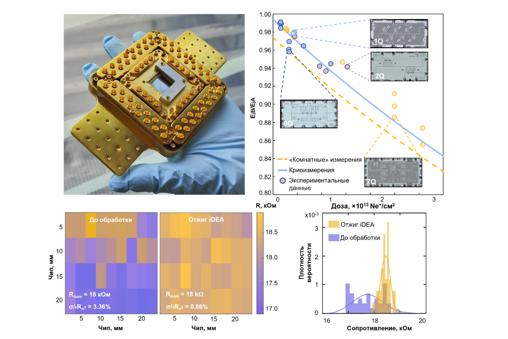
Russia’s iDEA technology (ion beam-induced DEfects Activation), developed at Shukhov.Nano, allows the formation of qubit elements using tunnel dielectrics just 0.8–2 nm thick with ±0.2 Å precision. This is made possible by a new physical mechanism for controlling dielectric thickness: when bombarded with ions, targeted defects are created in the crystal lattice, enabling ultra-precise tuning of the metal-oxide interface—critical for practical quantum computing.
One of the main barriers to useful quantum computing is the error rate in two-qubit operations, often caused by slight mismatches in qubit frequencies. If the energy levels of qubits and circuit elements align unintentionally, it causes crosstalk, leading to energy loss and computational errors. As qubit counts rise, these errors increase exponentially.
“Identical atoms used to be nature’s domain alone. Even small variations—±5 nm in size or sub-nanometer in tunnel barrier thickness—rendered some qubits unusable,” said Ilya Rodionov, head of Quantum Park. “A quantum processor integrates top-tier technologies, each of which must perform flawlessly. Our method enables critical control of qubit parameters—a major step toward practical quantum computing.”
Qubit frequency is set by the tunnel dielectric in the Josephson junction. Even atomic-level deviations shift frequencies, disrupting system behavior and reducing accuracy. iDEA allows tuning dielectric thickness at sub-ångström levels using helium or neon ion beams to modify the crystal structure precisely. The process is automated and takes just one second per qubit.
“This process is pre-calculated at the molecular level,” said Nikita Smirnov, lead developer of superconducting quantum processors at Quantum Park. “We tune each qubit to the target frequency, achieving deviations no greater than ±0.35%, which brings yield rates of quantum circuits close to 100%.”
Scalable Quantum Chips with 1000+ Qubits
The serial version of the technology enables tuning qubit frequencies over a 10 to 400 MHz range (0.2–10% variance). Maintaining a 0.35% (±17 MHz) frequency spread across a chip with local treatment areas under 10 nm is currently only possible with iDEA. The method doesn’t degrade qubit coherence, and the most coherent transmon qubits in Russia—made using iDEA—have lifetimes exceeding 500 µs, comparable to top global standards.
The technique has been tested in superconducting quantum coprocessors that successfully ran materials science algorithms.
IBM Quantum estimates that its current fabrication precision (±14–18 MHz) limits it to chips with ~300 qubits. The iDEA method is already demonstrating the feasibility of ±10 MHz precision. Moreover, the VNIIA/BMSTU architecture has looser frequency constraints, potentially enabling 1000+ qubit processors with near 99% yield.
Global First in Focused Ion Beam Atom Processing
This is the first time focused ion beam processing of artificial atoms has been proposed globally. Competing hybrid coprocessor developers use laser annealing, electron irradiation, or electrical treatments—methods that act over much larger areas and cannot selectively process nearby nanoscale features. iDEA is faster (1 second per qubit), more precise, and causes less damage than competitors like IBM Quantum (tens of seconds) or Rigetti (hundreds of seconds).
Beyond Quantum
The iDEA technology can also be applied to other post-CMOS processors that rely on hidden dielectric layers, including transistors, memristors, and magnetic skyrmions—key components for next-gen computing and AI systems. The method paves the way for practical use of post-CMOS architectures, essential for overcoming the physical and energy limits of conventional semiconductor processors.
The international scientific community has taken notice: the research results were published by Science Advances, and the collaboration between BMSTU and VNIIA has placed Russia among global leaders in post-CMOS technology