Insider Brief
- MIT researchers have developed a photonic chip that performs all the key operations of a deep neural network using light, enabling faster and more energy-efficient AI computations.
- The chip integrates optics and electronics to perform nonlinear operations directly on the chip, eliminating the need for external processors and reducing energy consumption.
- Capable of training AI models in real time, the chip achieves performance comparable to traditional hardware while completing computations in less than half a nanosecond.
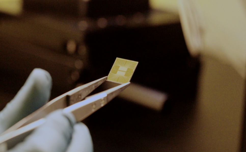
Scientists at MIT have developed a photonic chip that uses light to perform all the key operations of deep neural networks, potentially transforming how artificial intelligence computations are performed with unprecedented speed and efficiency, according to a story in MIT News.
As machine-learning models grow more complex, traditional processors struggle to keep up with their energy demands and computational requirements, the researchers report in their Nature Photonics paper. MIT’s photonic processor offers a solution by processing data using light rather than electricity. The chip achieves performance comparable to conventional processors while consuming less energy and completing computations in less than half a nanosecond.
“This is especially useful for systems where you are doing in-domain processing of optical signals, like navigation or telecommunications, but also in systems that you want to learn in real time,” said Saumil Bandyopadhyay, the study’s lead author and visiting scientist at MIT’s Research Laboratory of Electronics, as reported in MIT News.

Combining Optics and Electronics
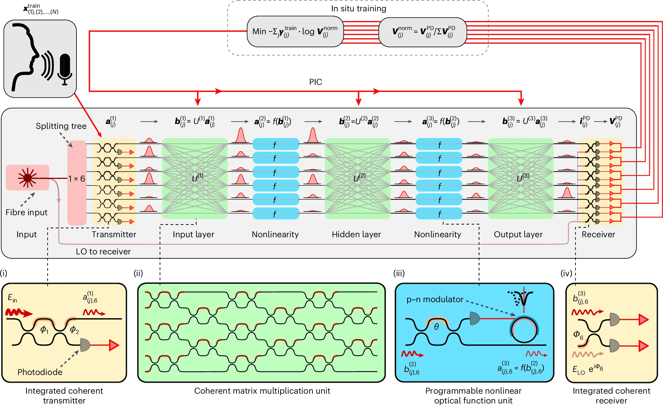
Deep neural networks rely on two key processes: linear operations like matrix multiplication and nonlinear operations that allow the network to learn complex patterns. While earlier optical chips could perform the linear calculations, they required external electronic processors for nonlinear tasks, adding inefficiencies.
MIT’s team overcame this limitation by creating nonlinear optical function units (NOFUs), small devices that integrate optics and electronics on the same chip, according to the article. These units convert a fraction of the light into electrical signals to perform nonlinear calculations without external amplifiers. This innovation ensures that computations stay mostly within the optical domain, enabling ultra-fast processing and low energy consumption.
Real-Time Learning on a Chip
One of the chip’s main features is its ability to train neural networks in real time — a process known as in situ training. Unlike traditional digital processors, which require significant energy to train AI models, the photonic chip handles this efficiently, making it ideal for applications where quick, on-the-spot learning is essential.
“This work demonstrates that computing — at its essence, the mapping of inputs to outputs — can be compiled onto new architectures of linear and nonlinear physics that enable a fundamentally different scaling law of computation versus effort needed,” Dirk Englund, senior author of the study and a professor at MIT’s Department of Electrical Engineering and Computer Science, told MIT News.
During testing, the chip achieved over 96% accuracy while training and more than 92% accuracy during inference, results that rival state-of-the-art electronic hardware.
Scaling for Real-World Use
The chip was fabricated using commercial foundry techniques, the same processes used to produce traditional CMOS computer chips. This approach could pave the way for large-scale manufacturing, allowing the technology to be integrated into everyday devices like cameras, lidar systems, and telecommunications networks.
“There are a lot of cases where how well the model performs isn’t the only thing that matters, but also how fast you can get an answer. Now that we have an end-to-end system that can run a neural network in optics, at a nanosecond time scale, we can start thinking at a higher level about applications and algorithms,” said Bandyopadhyay. The photonic processor’s nanosecond-scale speed positions it as a strong candidate for applications demanding rapid computations, from scientific research in particle physics to high-speed data transmission.
Future Directions
While the chip represents a significant step forward, researchers aim to further refine the technology. Next steps include scaling the device to handle more complex tasks and integrating it with existing electronics. The team is also exploring algorithms tailored to optical systems, which could enhance both training speed and energy efficiency.
The research was funded by the U.S. National Science Foundation, the U.S. Air Force Office of Scientific Research, and NTT Research. Collaborators included experts from MIT, NTT Research, and institutions specializing in quantum photonics and artificial intelligence.
For a more technical look at the research, please see the paper in Nature Photonics.


