
Quantum information systems promise faster and more powerful computing than traditional methods but scaling them to larger sizes and interconnecting multiple systems has been a significant challenge. Researchers at the University of Chicago’s Pritzker School of Molecular Engineering (PME) have made a breakthrough by combining two key technologies: trapped atom arrays and photonic devices. This innovation allows for the construction of larger, easily scalable quantum systems by using photonics to interconnect individual atom arrays.
Assistant Professor Hannes Bernien and his team developed a new chip geometry that enables atom arrays to interface with photonic chips without disrupting the fragile quantum states. In this setup, quantum computations are performed in one region, and specific atoms are moved to another region where they interact with photonic devices to extract data in the form of photons. These photons can then be transmitted through optical fibers, allowing for the interconnection of multiple atom arrays to create a larger quantum computing platform.
The new system also supports the simultaneous connection of multiple nanophotonic cavities to a single atom array, potentially leading to faster computation. While the team has demonstrated the feasibility of this approach, future studies will focus on photon collection and generating entanglement over long distances.
“Connecting atom arrays to photonic devices had been quite challenging because of the fundamental differences in the technologies. Atom array technology relies on lasers for their generation and computation,” said Shankar Menon, a PME graduate student and co-first author of the new work. “As soon as you expose the system to a semiconductor or a photonic chip, the lasers get scattered, causing problems with the trapping of atoms, their detection, and the computation.”

Co-first author Noah Glachman, a PME graduate student, explained that the chip design features two separate regions for atom movement — one located away from the photonic chip for computation and another near the photonic chip for interconnecting multiple atom arrays. He noted that this design minimizes interaction with the computational region of the atom array.
Menon added that the system could support hundreds of nanophotonic cavities simultaneously, all transmitting quantum information at once. This, he said, results in a significant increase in the speed of information sharing between interconnected modules.
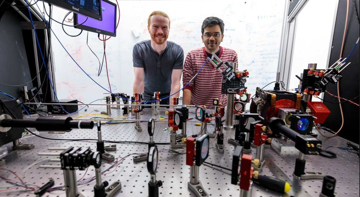
Featured image: Researchers in Bernien Lab, including graduate students Noah Glachman (left) and Shankar Menon, have discovered how to combine two powerful technologies — trapped atom arrays and photonic devices — to yield advanced systems for quantum computing, simulation, and networking. Credit: John Zich