
Researchers at Berkeley Lab and collaborating institutions have developed a novel approach to discover materials for quantum applications. The study, published in Nature Communications, combines theoretical computation with experimental validation.
“For defects to work for quantum applications, they need to have very specific electronic properties and structures,” said Geoffroy Hautier, a Dartmouth materials scientist and the project’s lead investigator. “They should preferably be able to absorb and emit light with wavelengths in the visible or telecommunications range.”
“Consider the material tungsten disulfide (WS2),” said Sinéad Griffin, a Berkeley Lab scientist and one of the study’s principal investigators. “If you account for the dozens of periodic table elements that could be inserted into this material and all the possible atomic locations for the insertion, there are hundreds of possible defects that could be made. Looking beyond WS2, if you consider thousands of possible materials for defects, there are literally infinite possibilities.”
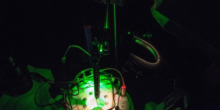
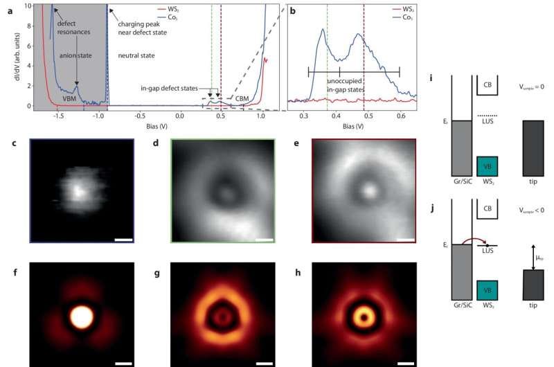
The team used high-throughput computational methods to screen over 750 defects in 2D tungsten disulfide (WS2), identifying a cobalt substitution as particularly promising. They then experimentally fabricated and examined this defect using atomic-level precision techniques at the Molecular Foundry.

“The microscope’s tip can see individual atoms and push them around,” said John Thomas, a Berkeley Lab postdoctoral researcher who conducted the fabrication. “It allows us to select a specific location for the cobalt atom and match the structure of the defect identified in the computational analysis. We’re essentially playing with atoms like LEGO bricks.”
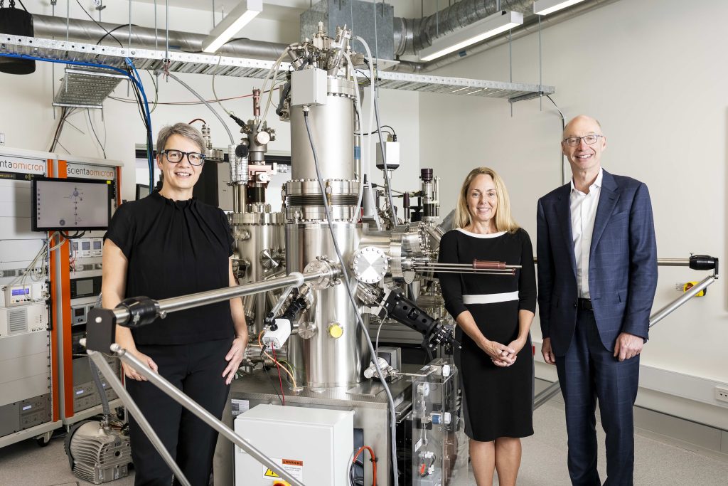
“This critical result shows the effectiveness of combining our computation and fabrication approaches to identify defects with sought-after properties,” said Weber-Bargioni. “It points to the value of using these approaches in the future.”
This approach reverses the traditional experimental-first method, significantly accelerating the discovery process. “In our approach, theoretical screening guides the targeted use of atomic-scale fabrication,” said Alex Weber-Bargioni, one of the study’s principal investigators and a scientist at Berkeley Lab’s Molecular Foundry, where much of this research was conducted. “Together, these methods open the door for researchers to accelerate the discovery of quantum materials with specific functionalities that can revolutionize computing, telecommunications, and sensors.”
The researchers have shared their findings in a public database called the Quantum Defect Genome to encourage further contributions from the global research community.
“Many factors came together to make this study a success,” said Hautier. “In addition to the computation and fabrication methods, our secret sauce was how the theorists and experimentalists collaborated. We met regularly and gave each other constant feedback on our methods to optimize the overall study. This deep collaboration was enabled by having common funding for the entire team.”
The study demonstrates the potential of combining theoretical prediction with precise experimental fabrication to advance quantum information science. “The ability to build complex materials with atomic precision — driven by theory — allows us to highly optimize their properties and potentially discover material functionalities that we do not even have a name for today,” said Weber-Bargioni. “We have built ourselves a huge materials playground for us to play in.”
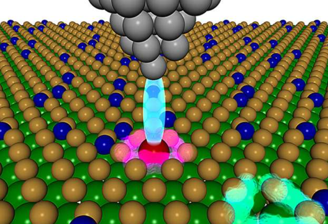
Featured image: This image shows the cobalt defect fabricated by the study team. The green and yellow circles are tungsten and sulfur atoms that make up a 2D tungsten disulfide sample. The dark blue circles on the surface are cobalt atoms. The lower-right area highlighted in blue-green is a hole previously occupied by a sulfur atom. The area highlighted in reddish-purple is a defect — a sulfur vacancy filled with a cobalt atom. The scanning tunneling microscope (gray) is using electric current (light blue) to measure the defect’s atomic-scale properties. Credit: John C. Thomas/Berkeley Lab