
Insider Brief
- University of Chicago’s Pritzker School of Molecular Engineering (PME) researchers have discovered how to combine trapped atom arrays and photonic devices to yield advanced quantum systems.
- They report in Nature that this could pave the way for large quantum systems which can be scaled up.
- The team is planning future studies that look at other steps in the process.
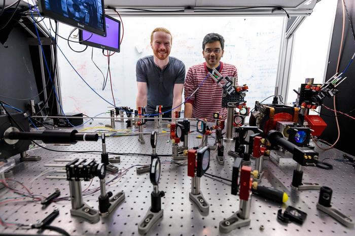
- Image: Researchers in Bernien Lab, including graduate students Noah Glachman (left) and Shankar Menon, have discovered how to combine two powerful technologies—trapped atom arrays and photonic devices—to yield advanced systems for quantum computing, simulation, and networking. (Photo by John Zich)
PRESS RELEASE — Quantum information systems offer faster, more powerful computing methods than standard computers to help solve many of the world’s toughest problems. Yet fulfilling this ultimate promise will require bigger and more interconnected quantum computers than scientists have yet built. Scaling quantum systems up to larger sizes, and connecting multiple systems, has proved challenging.
Now, researchers at the University of Chicago’s Pritzker School of Molecular Engineering (PME) have discovered how to combine two powerful technologies—trapped atom arrays and photonic devices—to yield advanced systems for quantum computing, simulation and networking. The new combination will allow the construction of large quantum systems which can be easily scaled up, by leveraging photonics to interconnect individual atom arrays.
“We have merged two technologies which, in the past, have really not had much to do with each other,” said Hannes Bernien, Assistant Professor of Molecular Engineering and senior author of the new work, published in Nature Communications. “It is not only fundamentally interesting to see how we can scale quantum systems in this way, but it also has a lot of practical applications.”

Arrays of neutral atoms trapped in optical tweezers—highly focused laser beams that can hold the atoms in place—are an increasingly popular way of building quantum processors. These grids of neutral atoms, when excited in a specific sequence, enable complex quantum computation that can be scaled up to thousands of qubits. However, their quantum states are fragile and can be easily disrupted—including by photonic devices that aim to collect their data in the form of photons.
“Connecting atom arrays to photonic devices had been quite challenging because of the fundamental differences in the technologies. Atom array technology relies on lasers for their generation and computation.” said Shankar Menon, a PME graduate student and co-first author of the new work. “As soon as you expose the system to a semiconductor or a photonic chip, the lasers get scattered, causing problems with the trapping of atoms, their detection and the computation.”
In the new work, Bernien’s group developed a new semi-open chip geometry allowing atom arrays to interface with photonic chips, overcoming these challenges. With the new platform, quantum computations can be carried out in a computation region, and then a small portion of those atoms containing desired data are moved to a new interconnect region for the photonic chip integration.
“We have two separate regions that the atoms can move between, one away from the photonic chip for computation and another near the photonic chip for interconnecting multiple atom arrays,” explained co-first author Noah Glachman, a PME graduate student. “The way this chip is designed, it has minimal interaction with the computational region of the atom array.”
In the interconnect region, the qubit interacts with a microscopic photonic device, which can extract a photon. Then, the photon can be transmitted to other systems through optical fibers. Ultimately, that means that many atom arrays could be interconnected to form a larger quantum computing platform than is possible with a single array.
An additional strength of the new system—which could lead to especially speedy computation abilities—is that many nanophotonic cavities can be simultaneously connected to one single atom array.
“We can have hundreds of these cavities at once, and they can all be transmitting quantum information at the same time,” said Menon. “This leads to a massive increase in the speed with which information can be shared between interconnected modules.”
While the team showed the feasibility of trapping an atom and moving it between regions, they are planning future studies that look at other steps in the process, including collection of the photons from the nanophotonic cavities, and the generation of entanglement over long distances.