
Insider Brief
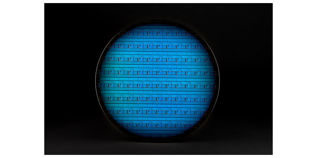
- Intel researchers report they developed a 300-millimeter (mm) cryogenic probing process to assess spin qubit devices across entire wafers.
- The process, an advance in the testing of spin qubit devices, is a step toward mass production and continued scaling of silicon-based quantum processors.
- The process provides high-volume data on spin qubit devices, demonstrating uniformity, fidelity and measurement statistics on spin qubits.
Intel’s Foundry Technology Research division has developed a 300-millimeter (mm) cryogenic probing process to assess spin qubit devices across entire wafers. The process provides high-volume data on spin qubit devices, demonstrating uniformity, fidelity and measurement statistics on spin qubits.
The researchers, who published their findings in Nature, report this represents an important step for the quantum computing industry, paving the way for the mass production and continued scaling of silicon-based quantum processors, according to a blog post written by an Intel researcher.
“Intel is taking steps toward building fault-tolerant quantum computers by improving three factors: qubit density, reproducibility of uniform qubits, and measurement statistics from high volume testing,”writes Sam Neyens, a quantum computing Research Engineer at Intel Foundry Technology Research.
Enhancing Quantum Testing and Production
Intel’s 300-mm cryogenic probing process is an advance in the testing of spin qubit devices by allowing testing across entire wafers, according to the post. The researchers demonstrated that single-electron devices perform exceptionally well as spin qubits, achieving 99.9% fidelity through CMOS manufacturing. The high fidelity and device yield streamline the path from fabrication to the study of spin qubits, a key development in scaling quantum computers.
Becuase spin qubits are small, measuring about 100 nanometers across, they are denser than other qubit types, such as superconducting qubits. If a single chip can house more qubits — because the qubits are denser — it can perform more quantum computations, making the chip more powerful and efficient.
Intel’s most recent work addresses three key areas essential to advancing quantum computing: qubit density, reproducibility, and high-volume testing. The company’s silicon spin qubits are smaller and denser than other types, including superconducting and trapped ion qubits. This density is made possible by Intel’s EUV lithography, which, in conjunction with high-volume manufacturing, supports large-scale production. Intel’s 300-mm CMOS manufacturing methods also ensure the reproducibility and reliability needed for fabricating millions of uniform qubits.
The cryogenic probing system accelerates testing by offering a process that gathers data much faster than traditional singular device testing.
“Intel’s entire testing process, from alignment to device measurement, is fully automated and programmable, speeding up device data collection by several orders of magnitude compared with the measurement of singular devices in a cryostat,” Neyens writes.
Bluefors AEM Collaboration
The collaboration with Bluefors and AEM Afore has resulted in a cryoprober capable of cooling 300-mm wafers to 1 Kelvin at the chuck, allowing comprehensive testing of spin qubit devices across the wafer. The wafer probe can cool devices to a base temperature of 1 K in two hours, providing consistent and comprehensive feedback.
Intel’s manufacturing process has led to improved charge noise, interdot coupling, and overall disorder, which the researchers stress are essential for stable spin qubit operation.
Researchers have also optimized the process by testing 12QD devices across wafers, analyzing the yield of ohmic contacts, gates, quantum dots, and full devices. This optimization has led to higher yield and lower variation, akin to leading-edge technology nodes.
According to a statement from Intel, more work remains.
The company states: “Building on these findings, Intel plans to continue to make advances in using these techniques to add more interconnect layers to fabricate 2D arrays with increased qubit count and connectivity, as well as demonstrating high-fidelity two-qubit gates on its industry manufacturing process. However, the main priority will continue to be scaling quantum devices and improving performance with its next generation quantum chip.”