
Insider Brief:
- A University of Washington research team led by Arka Majumdar has made significant strides in quantum simulation technology, demonstrating a new kind of silicon photonic chip as a potential foundation for building quantum simulators, which have real-world application potential, particularly in medical research for simulating complex molecular interactions.
- The silicon photonic chip, fabricated at the Washington Nanofabrication Facility, presents a scalable, measurable, and programmable solution, overcoming three of the four major challenges in quantum simulator development.
- This technology is seen as a more feasible and cost-effective approach compared to other quantum simulation platforms, owing to its compatibility with existing silicon fabrication processes used in semiconductor chip production.
The domain of superconducting system design and fabrication has witnessed notable progress, culminating in the successful creation of several prototypical quantum simulators exemplifying small-scale quantum systems. Yet, scaling these systems to a usable size presents a challenge, alongside operational hurdles encountered when attempting to utilize superconducting systems for the simulation of actual quantum materials.
However, advancements in quantum simulation have been significantly propelled forward by a research team from the University of Washington, under the leadership of Arka Majumdar, an associate professor with expertise in physics as well as electrical and computer engineering at UW. Through a demonstration published in Nature Communications, the team illustrated that a novel silicon photonic chip has the potential to serve as a robust foundation for constructing a quantum simulator with practical applications in the real world.
Specializing in optics, photonics, and quantum technologies development, Majumdar holds a distinguished position at UW. Besides his teaching and research duties, he serves as a co-chair of QuantumX and is affiliated with the Institute for Nano-Engineered Systems.
“We’ve shown that photonics is a leading contender for quantum simulation, and photonic chips are a reality,” said Majumdar. “We believe that these chips can play a very important role in building a quantum simulator.”
Abhi Saxena, lead author of the paper and recent UW ECE alumnus who graduated in 2023 with his doctoral degree and now works for the National Institute of Standards and Technology (NIST) in Boulder, Colorado, added: “This is a very good platform for realizing a useful quantum simulator that could be scaled to large sizes.”
The research team also comprises Arnab Manna, who is pursuing a doctorate in the physics department, and UW ECE Assistant Professor Rahul Trivedi. Trivedi, with his expertise in quantum systems, provided assistance on the theoretical facets of the research.
Photonics, a subset of optics focusing on the behaviour and properties of light, encompasses the generation, detection, and manipulation of light, facilitating various technologies like lasers, fibre optics, and light-emitting diodes (LEDs). One notable benefit of using photonics for crafting a quantum simulator platform is the ability to fabricate photonic devices in CMOS foundries, which have a long-standing history of manufacturing semiconductor chips.
“The fabrication process that we have for this chip can directly latch onto the already well-matured silicon fabrication that we do for transistors and other computer chips,” said Saxena. “Whereas for other quantum simulator platforms that’s not feasible, even though many of them have already demonstrated prototypical devices.”
The research team fabricated their silicon photonic chip at the Washington Nanofabrication Facility located on the UW campus, exemplifying a production method that not only aims to reduce the manufacturing costs of a quantum simulator but also holds promise in scaling up the chip for utilization across a broad spectrum of quantum simulation devices.
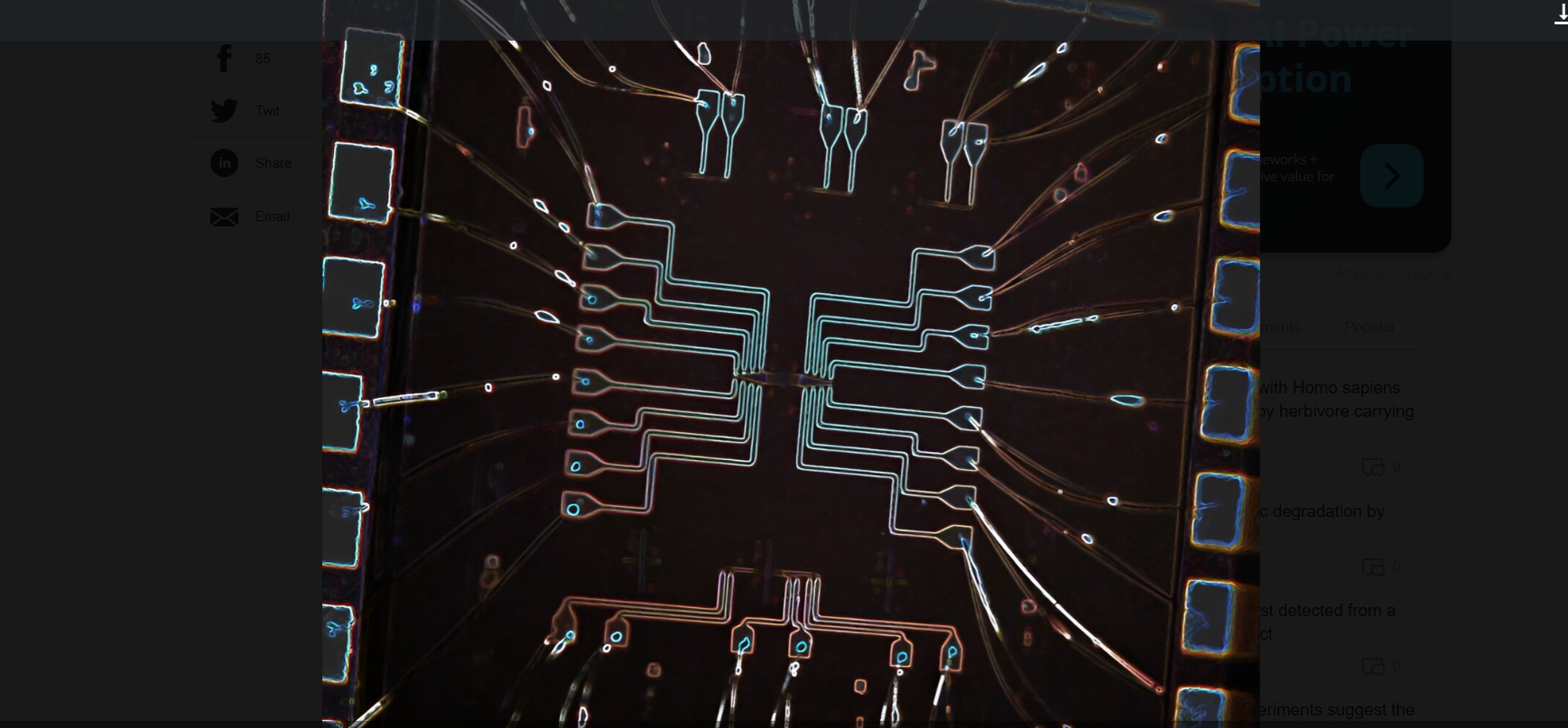
Central to the design of the chip is an array termed as “photonic coupled cavity array.” This array, composed of eight photonic resonators, represents a pseudo-atomic lattice and acts as a realm where photons can be securely housed, their energy levels adjusted, and maneuvered in a regulated fashion, essentially constructing circuits.
The team introduced pivotal technical advancements concerning the array. Firstly, they devised a mathematical algorithm enabling detailed characterization, or mapping of the chip, utilizing only the data accessible on the chip’s peripheries. Secondly, they pioneered a novel architectural design for heating and individually managing each cavity within the array, thereby facilitating the programming of the device. Per Majumdar and Saxena, such innovations, realized on a silicon photonic chip, mark a first in this domain.
“We are demonstrating everything on a chip, and we have shown scalability, measurability and programmability — solving three of the four major obstacles to using a silicon photonic chip as a platform for a quantum simulator,” said Majumdar. “Our solution is a small size, it is not misalignment-prone, and we can program it.”
The research team aims to overcome the final significant hurdle towards constructing a fully realized quantum simulator by inducing a condition termed “nonlinearity.” Unlike the inherent repulsion between electrons due to their negative charge in electronic circuits, photons naturally don’t interact with each other. Achieving a similar interaction within a quantum simulator is crucial to establishing nonlinearity and completing the circuitry, and the team is exploring various methodologies to resolve this. Additionally, they are working on refining their silicon photonic chip to comply with standard chip foundries, enabling global manufacturing at semiconductor fabrication facilities. While Majumdar and Saxena acknowledge this development as a comparatively less challenging obstacle, they remain optimistic about the potential global impact of their chip.
“Through this work, we presented a solid foundation for a platform that demonstrates photonics and the semiconductor-based technology we are using as viable alternatives to create quantum simulators,” said Saxena. “I think that up until now, many in the scientific and engineering communities have generally avoided considering photonics for this purpose. But our work shows that it is realistically possible, so it is a very good incentive for more people to begin moving in this direction.”
Featured image: An optical image of the electrically controlled coupled cavity array in the team’s silicon photonic chip. The image depicts the wiring structure and optical micrograph of the coupled cavity array. This visual, provided by Abhi Saxena, is an edge detected output that uses an optical microscope image as an input. Credit: University of Washington
If you found this article to be informative, you can explore more current quantum news here, exclusives, interviews, and podcasts.