Insider Brief
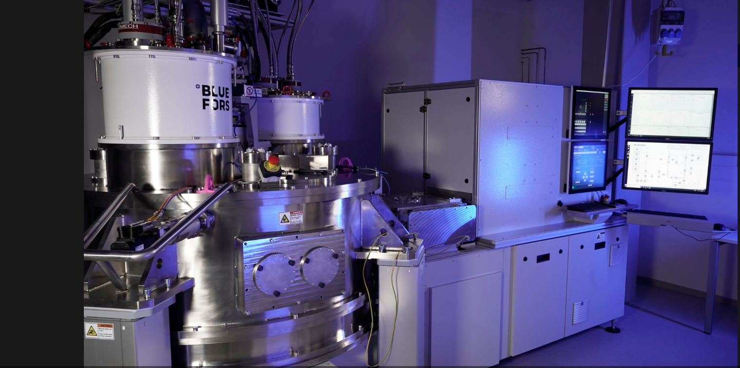
- Germany has introduced its first cryogenic measurement system for assessing qubit device quality, a groundbreaking development taking place at the renowned Fraunhofer Institute for Applied Solid State Physics IAF.
- This innovative on-wafer prober stands out due to its ability to scrutinize qubit devices based on various technologies, including semiconductor quantum dots, quantum wells, and superconductors, all at extremely low temperatures below 2 Kelvin. Its full automation promises to build a substantial and valuable database, revolutionizing high-quality quantum device production in Europe.
- The successful completion of the KryoproPlus project and the inauguration of the wafer prober mark a significant achievement for the Fraunhofer IAF. This institution’s dedication to pushing the boundaries of quantum research and technology is shaping the future of quantum computing and sensing, solidifying its position as a pioneering force in the quantum technology landscape.
Germany has unveiled its first-ever cryogenic measuring setup for assessing the quality of qubit devices. Nestled within the esteemed Fraunhofer Institute for Applied Solid State Physics IAF, this groundbreaking on-wafer prober is set to revolutionize the way we perceive and harness the power of quantum phenomena.
Super Cold
What sets this innovation apart is its ability to scrutinize qubit devices based on semiconductor quantum dots, quantum wells, and superconductors, all at measurement temperatures plummeting below 2 Kelvin, which translates to a bone-chilling -271.15 degrees Celsius. This cryogenic marvel comes equipped with full automation, enabling researchers to embark on an ambitious journey to compile a vast, quantitatively relevant database that promises to redefine the landscape of high-quality quantum device production across Europe.
At the heart of this is the aspiration to unravel the intricate workings of quantum devices. With the ability to characterize wafers on an industrial scale (ranging from 200 mm to 300 mm) and process them in substantial quantities (up to 25 wafers in succession), this on-wafer prober is set to usher in a new era of discovery. By generating comprehensive datasets that mitigate the inherent variability found in single measurements, the Fraunhofer Institute’s cryogenic setup stands as a beacon of hope, driving us closer to the realization of dependable, high-quality qubits poised for integration into quantum computers and quantum sensors.
Remarkably, this pioneering facility marks the fifth of its kind on a global scale, the second within Europe, and most notably, the first of its kind in Germany. This was made possible through funding from the German Federal Ministry of Education and Research (BMBF) as part of the visionary “KryoproPlus — Provision and Verification of a Cryogenic On-Wafer Prober” project. With this new tool at their disposal, Germany’s quantum researchers are primed to explore uncharted frontiers, paving the way for a quantum-powered future that promises to transcend the boundaries of today’s computing capabilities.
Unique Capabilities
“With the on-wafer prober we gain new and unique capabilities in cryogenic characterization nationwide,” said Prof. Dr. Rüdiger Quay, KryoproPlus project coordinator and acting institute director of Fraunhofer IAF.
“With this system, we will support our partners from research and industry in establishing a European supply chain for materials and production processes for solid-state qubits. This allows us to make an important contribution to the technological sovereignty of Germany and Europe,” added Quay.
“The wafer prober provides us for the first time with statistically relevant data sets that we can use to systematically optimize and scale the production of qubit devices,” said Nikola Komerički, who is supervising the KryoproPlus project as part of his doctorate on the characterization of quantum computing devices. Komerički coordinated the installation and commissioning of the system and is already performing the first measurements.
“We want to better understand how to get good, homogeneous qubits to enable scaling and industrial production of qubits in Germany and Europe,” added Komerički. “To do that, it is necessary to expand the qualitative view to include a quantitative, statistical perspective on device behaviour.”
Quantum bits (qubits) that rely on semiconductor quantum dots, quantum wells and superconductors function at temperatures nearing absolute zero, a frosty -273.15 degrees Celsius. This frigid environment serves a triple purpose: it quashes ambient interference, triggers superconductivity and paves the way for the creation and entanglement of these enigmatic qubits. Consequently, achieving precision in the testing, fine-tuning, and expansion of qubit technology mandates thorough characterization at their operational cryogenic temperature, complemented by the accumulation of statistically significant measurement data.
Enter the cryogenic on-wafer prober, a technological marvel that effectively bridges this characterization chasm. Operating in a fully automated fashion, it measures entire 200 mm and 300 mm wafers, all while maintaining temperatures below the frosty threshold of 2 Kelvin. This exceptional feat drastically amplifies the reservoir of accessible data, endowing researchers and engineers with a solid foundation to embark on purposeful enhancements for qubit-forming instruments and, in turn, elevate the prospects of scalability. In essence, this innovation empowers the quantum frontier with the vital tools needed to propel qubit technology to new heights.
KryoproPlus Project
The successful inauguration of the wafer prober marks the triumphant conclusion of the KryoproPlus project, a momentous achievement in the realm of quantum exploration. This cutting-edge facility has embarked on its maiden measurements as part of three groundbreaking initiatives: “MATQu — Exploring Quantum Materials,” “QUASAR — Pioneering Semiconductor Quantum Processor with Scalable Shuttling Architecture,” and “QLSI — Revolutionizing Large-Scale Quantum Integration with Silicon.”
Within the domain of MATQu, the mind of Komerički delves into the intricate world of (niobium) Josephson junctions, crucial components for transmon qubits. Meanwhile, over in the realms of QUASAR and QLSI, meticulous characterizations unfold, focusing on field-effect transistors (FETs) catering to single-electron transistors (SETs) grounded in silicon quantum wells. These initial steps pave the way for the eventual creation of SETs that function as the bedrock for pioneering spin qubit devices. In essence, these undertakings are key milestones propelling us further into the captivating realm of quantum computing.
The Fraunhofer Institute for Applied Solid State Physics IAF has emerged as a pioneering force in the quantum technology landscape, and its recent achievement in establishing the cryogenic on-wafer prober marks a significant leap forward. By pushing the boundaries of quantum research and technology, the institute has not only expanded our understanding of qubit devices but also played a crucial role in advancing the prospects of quantum computing and sensing. With their dedication to innovation and excellence, the Fraunhofer IAF continues to be at the forefront of shaping the quantum future, where limitless possibilities await.
Source material provided by Fraunhofer Institute for Applied Solid State Physics IAF
Featured image: The cryogenic on-wafer prober at Fraunhofer IAF enables fully automatic characterizations of up to 25 whole 200-mm or 300-mm wafers with devices for quantum computing and sensing. Credit: Fraunhofer IAF
For more market insights, check out our latest quantum computing news here.