
Insider Brief
- Researchers say they have demonstrated a more effective technique for creating quantum emitters using pulsed ion beams.
- The work was led by Department of Energy Lawrence Berkeley National Laboratory (Berkeley Lab).
- The team targeted the fabrication of a specific type of color center in silicon comprising two substitutional carbon atoms and a slightly dislodged silicon atom.
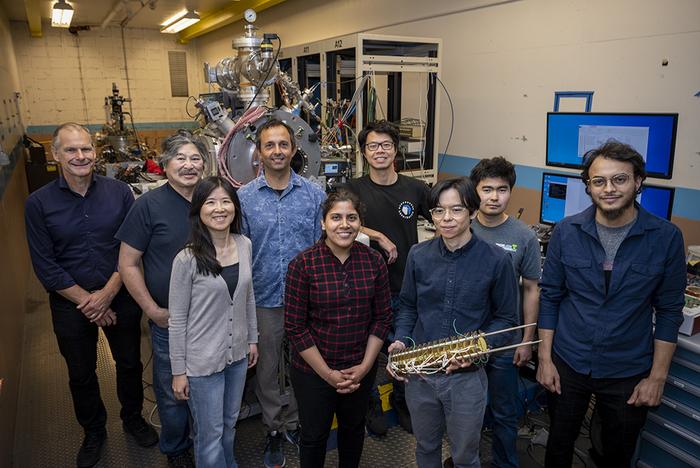
- Members of the team that conducted the research. Theory lead Liang Tan is holding one of the ion accelerators used to form quantum light emitters in silicon. (Left to right: Thomas Schenkel, Takeshi Katayanagi, Qing Ji, Arun Persaud, Kaushalya Jhuria, Wei Liu, Liang Tan, Yertay Zhiyenbayev, and Walid Redjem). Thor Swift/Berkeley Lab
PRESS RELEASE — The prospect of a quantum internet, connecting quantum computers and capable of highly secure data transmission, is enticing, but making it poses a formidable challenge. Transporting quantum information requires working with individual photons rather than the light sources used in conventional fiber optic networks. To produce and manipulate individual photons, scientists are turning to quantum light emitters, also known as color centers. These atomic-scale defects in semiconductor materials can emit single photons of fixed wavelength or color and allow photons to interact with electron spin properties in controlled ways.
A team of researchers has recently demonstrated a more effective technique for creating quantum emitters using pulsed ion beams, deepening our understanding of how quantum emitters are formed. The work was led by Department of Energy Lawrence Berkeley National Laboratory (Berkeley Lab) researchers Thomas Schenkel, Liang Tan, and Boubacar Kanté who is also an associate professor of electrical engineering and computer sciences at the University of California, Berkeley. The results appeared in Physical Review Applied and are part of a larger effort by the team to identify the best quantum defect emitters for processing and transporting quantum information and to produce them with precision.
“The color centers we’re making are candidates for becoming the backbone of a quantum internet and a key resource for scalable quantum information processing,” said Schenkel, a senior scientist in Berkeley Lab’s Accelerator Technology & Applied Physics (ATAP) Division. “They could support linking quantum-computing nodes for scalable quantum computing.”
In this work, the team targeted the fabrication of a specific type of color center in silicon comprising two substitutional carbon atoms and a slightly dislodged silicon atom. The conventional method of producing the defects is to hit the silicon with a continuous beam of high-energy ions; however, the researchers discovered that a pulsed ion beam is significantly more efficient, producing many more of the desired color centers.
“We were surprised to find these defects can be more easily generated with pulsed ion beams,” said Wei Liu, a postdoctoral scholar in ATAP and first author of the publication. “Right now, industry and academia mainly use continuous beams, but we’ve demonstrated a more efficient approach.”
The researchers believe that the transient excitations created by the pulsed beam, where the temperature and system energetics change rapidly, are key to the more efficient color center formation, which they established through an earlier study using pulsed ion beams from a laser-driven accelerator published in Communications Materials.
The team characterized the color centers at cryogenic temperatures using highly sensitive near-infrared detectors to probe their optical signals. They found that the intensity of the ion beam used to create the color centers changed the optical properties of the photons they emitted. Large-scale computer simulations on the Perlmutter system at the National Energy Research Scientific Computing Center (NERSC) provided further insight into the discovery, revealing that the wavelength of emitted photons is sensitive to strain in the crystal lattice.
“First-principles electronic structure calculations have become the go-to method for understanding defect properties,” added Vsevolod Ivanov, a postdoctoral scholar at the Molecular Foundry and co-first author of the publication. “We have reached the point where we can predict how a defect behaves, even in complex environments.”
The findings also suggest a new application for quantum emitter color centers as sensors for radiation.
“It opens new directions,” said Tan, a staff scientist at Berkeley Lab’s Molecular Foundry. “We can form this color center by just hitting silicon with a proton. We could potentially use that as a dark-matter or neutrino detector with directionality because we see these different strain fields depending on which way the radiation came.”
With this deeper understanding of quantum emitter formation and properties, the team continues to expand its exploration of color centers. Ongoing work includes generating a database of color centers predicted to exist in silicon, using computer simulations to identify those best suited to quantum computing and networking applications, and refining fabrication techniques to gain deterministic control over creating individual color centers.
“We’re working towards a new paradigm of qubits by design,” said Kanté. “Can we reliably make a given color center that operates in the telecom band, has sufficient brightness, isn’t too hard to make, has a memory, etcetera? We’re engaged in that quest and have demonstrated some exciting progress.”
“The new pathways to forming color centers using intense beams uncovered in this work are an exciting application of high energy density conditions and plasma science to improving technologies for quantum information science,” said ATAP Division Director Cameron Geddes.
The Molecular Foundry and National Energy Research Scientific Computing Center (NERSC) are DOE Office of Science user facilities located at Berkeley Lab.
This research was funded by the DOE Office of Science’s Fusion Energy Sciences and High Energy Physics programs.
If you found this article to be informative, you can explore more current quantum news here, exclusives, interviews, and podcasts.