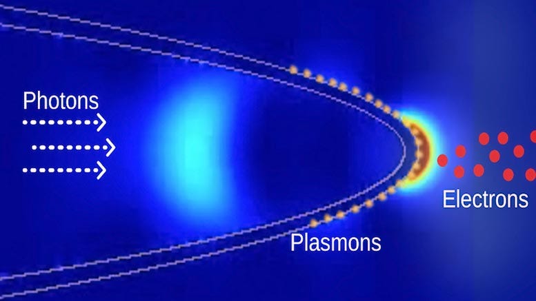
Surface Plasmons
Scientists at the Department of Energy’s Oak Ridge National Laboratory (ORNL) and the University of Nebraska have come up with a simpler way to create electrons that can be used for nanoscale imaging and sensing. By achieving this, it’s on its way to becoming an innovative tool in disciplines such as bioimaging and material science, not to mention in fundamental quantum technology research.
So what’s the secret?
Published in the New Journal of Physics, the study reported that shooting laser pulses (photons) through a fibre-optic nanotip caused the electrons in the tip into collective oscillations (surface plasmons) which forced the tip to discharge the electrons. This in turn produced an electron gun. These emitted electrons can be employed to scrutinize materials from all angles, and are undoubtedly much better than current technology in the field can achieve.
The group’s findings were documented in two papers published in August of this year, one Surface plasmon enhanced fast electron emission from metallised fibre optic nanotips (New Journal of Physics) and the second Photofield electron emission from an optical fiber nanotip (Applied Physics Letters).

Ali Passian of ORNL’s Quantum Information Science group and a co-author on both papers said: “It works on the principle of light activation, so light comes in and stimulates the electrons in the metal just in the right way for them to gain enough energy to come out.”
Electrons have a huge advantage over photons when it comes to probing the surface of materials. Having a shorter wavelength than light (photons), in turn they are able to magnify objects at nanometre resolution, much higher than what is currently available using light magnification. Just to put it into context, a nanometre is a billionth of a metre, so it just goes to show the potential power these nanotip electron guns have for existing and future deep-tech industries.

Before this study, nanotip emission methods relied on external light stimulation. To generate electrons, researchers were forced to accurately position laser beams onto the tip of the electron gun.
“Previously, lasers had to track the tips, which is technologically a much harder thing to do,” Herman Batelaan, another co-author on the study who leads electron control research at the University of Nebraska, said.
Future Uses
Such findings could be a blessing for industries where nanoscale imaging and sensing are required (biological or chemical sensing applications, for instance) to enhance the resolution and sensitivity of images whose ultimate goal is to treat diseases.
“To our knowledge this is the smallest laser intensity that has given rise to electron emission from nanotips.”
— Sam Keramati, postdoctoral researcher, University of Nebraska-Lincoln
In an era where human health outcomes are severely threatened by the likes of COVID-19 etc, biomedical applications like nanobiosensors could be improved upon due to the joint work of the Department of Energy’s Oak Ridge National Laboratory and the University of Nebraska fibre-optic nanotip electron gun.
If you found this article to be informative, you can explore more current quantum news here, exclusives, interviews, and podcasts.


