FBH Offers Diamond Processing For Quantum Technologies


Insider Brief
- FBH offers a diamond processing platform to develop nanoscale components for quantum communication, sensing and information processing.
- Customers can commission surface preparation, ion implantation to create color centers, and nanoscale pillar fabrication separately or in combination.
- The platform aims to establish reproducible, scalable processes and integrate diamond nanostructures with photonic circuits.
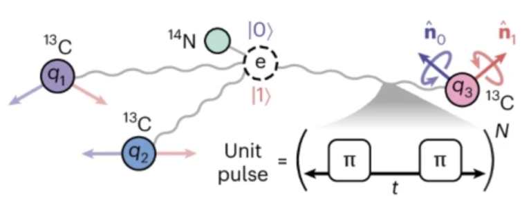
PRESS RELEASE — Diamond is attracting growing interest for quantum technologies. Defects in its crystal lattice, known as color centers, can behave like individual atoms. Their discrete spin states can be addressed through optical transitions, making them promising building blocks for quantum memories and light sources for quantum communication and sensing.
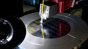
Translating these properties into functional devices, however, requires diamond itself to be processed with particularly high precision. Compared with established semiconductor technologies, nanostructuring of diamond remains relatively unexplored. At FBH, the Joint Lab Diamond Nanophotonics with Humboldt-Universität zu Berlin combines semiconductor process technology with expertise in quantum optics and solid-state nanosystems.
“With our diamond processing capabilities, we are establishing a technology platform that brings together precise nanofabrication and quantum optical functionality,” says Prof. Dr. Tim Schröder, head of the Joint Lab Diamond Nanophotonics. “This allows us to develop and refine processes for different color centers and make them available for research and application-oriented development.”

From surface preparation to nanoscale structures
FBH offers three complementary processing steps:
First, plasma etching prepares the diamond surface for further processing. Mechanical polishing can leave strain and damage near the surface, potentially introducing unwanted noise in quantum applications. The etching process removes this affected layer, creating a well-defined, low-damage surface. Using oxygen- and chlorine-based plasma etching, FBH can remove up to 20 µm of material while maintaining a surface roughness of around 0.5 nm rms.
Next, selected ions can be implanted into the diamond to create color centers. FBH can introduce different elements, including carbon, nitrogen, silicon, germanium and tin, to create specific color centers. Implantation into high-purity diamond substrates helps achieve color centers with low noise and good coherence. This controlled process is an important step towards efficient quantum memories and advanced sensing applications.
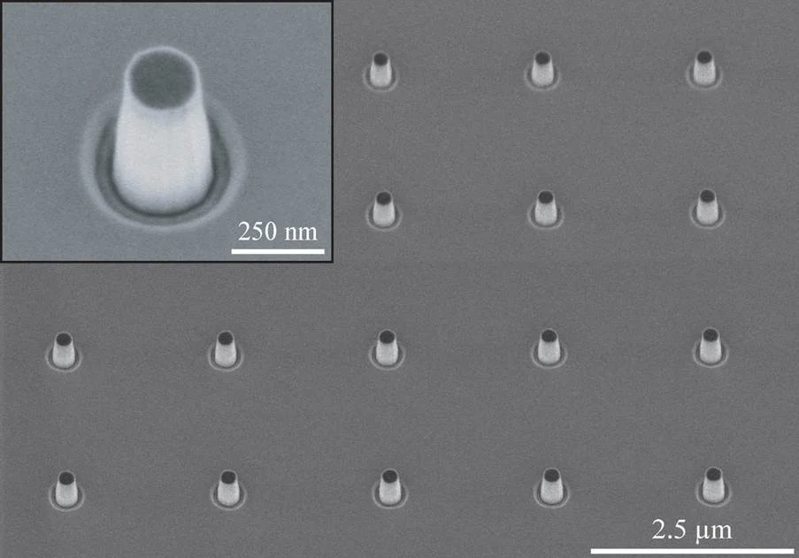
Finally, FBH can structure the diamond into nanoscale pillars. These structures can contain individual color centers and enhance the collection of the photons they emit, improving the efficiency of single-photon sources. They can also be used for quantum sensing and communication. Electron-beam lithography provides the flexibility that allows the geometry of the nanostructures to be tailored to specific applications.
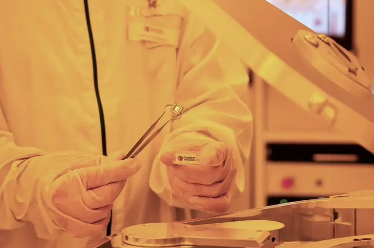
Customers can commission these processing steps separately or in combination. FBH can provide suitable diamond substrates or process material supplied by customers.
A platform for integrated quantum photonics
The processing platform builds on years of research into defect centers in diamond and FBH’s established expertise in nanofabrication. Its goal is to achieve reproducible, scalable processes and ultimately combine diamond nanostructures with photonic circuits.
The platform is designed to provide a toolbox for integrating established and emerging color centers into photonic systems. Possible applications range from bright, compact quantum light sources to spin-photon interfaces for quantum information processing, including entanglement operations and diamond-based sensors.
FBH and its research partners have already demonstrated key processing capabilities. In a study published in Physical Review X, the researchers demonstrated nitrogen-vacancy centers in diamond nanopillars with narrow optical linewidths. These included lifetime-limited linewidths measured on a one-second timescale and an inhomogeneous linewidth of 150 MHz: https://journals.aps.org/prx/
In further studies, collaborators investigated the optical and quantum properties of color centers implanted at FBH.
More information: https://www.fbh-berlin.de/en/

Keep track of everything going on in the Quantum Technology Market. In one place.
Topics

Matt Swayne
With a several-decades long background in journalism and communications, Matt Swayne has worked as a science communicator for an R1 university for more than 12 years, specializing in translating high tech and deep tech for the general audience. He has served as a writer, editor and analyst at The Quantum Insider since its inception. In addition to his service as a science communicator, Matt also develops courses to improve the media and communications skills of scientists and has taught courses.
[email protected]

Stay Ahead of Quantum
Get the latest research, company news, and market intelligence every week.
MENTIONED IN THE ARTICLE