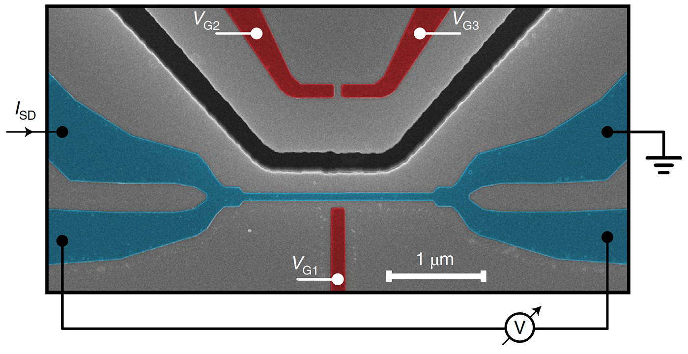
The scientists, who reported their findings in Nature Electronics, offered a new explanation for that the microscopic processes behind the functioning of a new superconducting switch, introduced in a 2018 paper. In those experiments, superconductivity in a metallic nanowire shut down after a moderate voltage was applied to a nearby gate electrode. That team suggested that the electric field associated with the voltage caused the superconductivity suppression, which would go against most of the current understanding of how electric fields affect superconductors and metals in general.
In a blog post, IBM researchers now have an alternative explanation: at the gate voltages where superconductivity was suppressed, weak currents of high-energy electrons leaking out of the gate were always present.
“In our latest paper, we provide an explanation of how just a relatively small number of those high-energy electrons are sufficient to disrupt the superconducting state in the nanowire,” the scientists write. “We realized a novel device geometry where a current of high energy electrons is generated without exposing the nanowire to electric fields or leakage currents. Instead, currents are produced in the vicinity of the nanowire by additional gate electrodes.”

According to the researchers, when a current flows among the two remote gates, the superconductivity in the nanowire is suppressed similar to when the nearby gate is used.
They explain: “In a first step, the high energy electrons trigger the emission of phonons in the silicon substrate on which both the nanowire and the gates sit. Like water waves, these phonons travel a considerable distance (several microns) and reach the superconducting nanowire, where they efficiently suppress superconductivity.”
These findings may lead to important advances in superconducting applications, including quantum ones, they added.
“Our findings, and specifically the role we now show phonons play, are critically important when designing devices for superconducting quantum applications,” the researchers write. “In fact, switches based on this effect would require very little power to work, and as such could be far more efficient than other methods, such as warming up a nanowire with resistive heating. In addition, our results suggest new strategies that could be used to mitigate the well-known negative impact of phonons on the coherence of superconducting qubits. A way to circumvent that detrimental effect of phonons could be by structuring the substrate — like we did with the trench — to attenuate, or confine, the impact of the emitted phonons.”
For more market insights, check out our latest quantum computing news here.


